
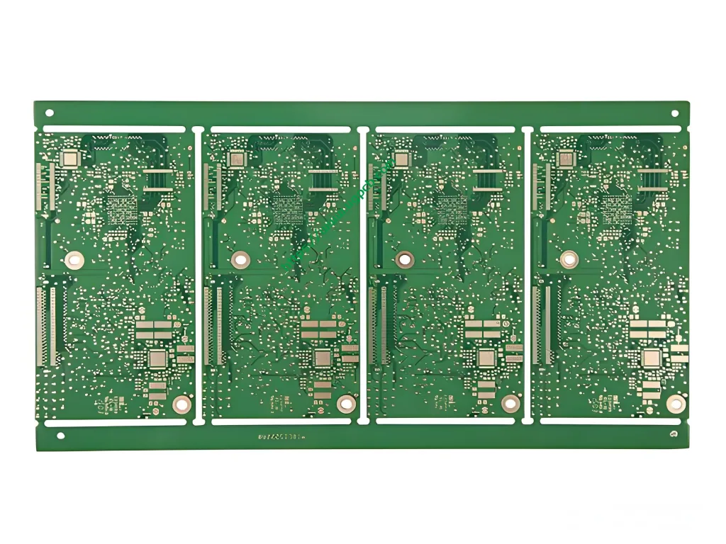
8-слойная печатная плата HDI 1+N+1 от UGPCB: Комплексное руководство
В неустанном стремлении к миниатюризации и повышению производительности в электронике, Взаимодействие высокой плотности (ИЧР) печатные платы стали краеугольным камнем. 8-уровневый продукт 1+N+1 HDI от UGPCB представляет собой сложное решение для дизайнеров, расширяющее границы возможного.. В этой статье представлен подробный обзор этого продвинутого печатная плата технология.
Что такое 8-слойная печатная плата 1+N+1 HDI?
8-слойная печатная плата 1+N+1 HDI представляет собой особый тип плата межсоединений высокой плотности. Номенклатура “1+N+1” описывает структуру наращивания микроотверстий.
-
Первая и последняя «1»: Они представляют собой один слой микроотверстий высокой плотности на верхней и нижней поверхностях платы.. Эти микроотверстия обычно создаются с помощью лазерного сверления..
-
Затем': Это представляет собой ядро платы., в данном случае это стандартный 6-слойный многослойная печатная плата (общая сумма 8 слои). Сердцевина содержит сквозные или скрытые переходные отверстия, соединяющие внутренние слои..
Такая структура позволяет обеспечить очень большое количество соединений в компактном пространстве., что делает его идеальным для сложных, ограниченный пространством Проекты печатных плат необходим для современной микроэлектронной продукции.
Основные конструктивные особенности и характеристики
UGPCB производит эту печатную плату HDI с высокой точностью., соблюдение следующих критических характеристик:
-
Материал: Высокий Tg FR-4, прочный и надежный ламинат, обладающий превосходной термической и механической стабильностью..
-
Толщина доски: Готовая толщина 0,8 мм., поддержка тонких профилей продуктов.
-
Медный вес: 1 унция (35мкм) для внутренних слоев и 0.5 унция (17.5мкм) для внешних слоев. Этот баланс обеспечивает хорошую пропускную способность по току, одновременно обеспечивая более тонкое травление следов внешнего слоя..
-
Поверхностная отделка: Погружение Золото (СОГЛАШАТЬСЯ) через OSP (Органическая припаяя консервант) фундамент. Эта комбинация обеспечивает ровную, прочная поверхность для пайки и отличный срок хранения.
-
Минимальный след/пространство: 3 мил (0.075 мм), создание схем высокой плотности.
-
Минимальный размер отверстия: 0.2мм для механических сверл и сверхтонкий 0,1 мм для микроотверстий, просверленных лазером..
Как работает структура печатной платы HDI
The “1+N+1” функции архитектуры, создавая более эффективный путь маршрутизации. Вместо использования больших сквозных отверстий, которые занимают ценную площадь на каждом слое., этот HDI дизайн печатной платы использует микроотверстия. Эти крошечные отверстия, просверленные лазером, соединяют только соседние слои. (например, от L1 до L2, или от L8 до L7). Этот “сложенный” или “пошатнулся” Через подход освобождает каналы маршрутизации на внутренних уровнях, что позволяет обеспечить гораздо большую плотность компонентов и более эффективные пути прохождения сигнала, что имеет решающее значение для высокоскоростного Сборка печатной платы.
Основные приложения и варианты использования
Основное применение этой усовершенствованной печатной платы HDI — сложные микроэлектронные продукты.. Конкретные варианты использования включают в себя:
-
Носимые технологии: Умные часы, фитнес-трекеры, и медицинские мониторы.
-
Передовые мобильные устройства: Смартфоны, таблетки, и ультрапортативные ноутбуки.
-
Медицинское оборудование высокой плотности: Миниатюрные медицинские устройства визуализации и диагностики.
-
Аэрокосмическая и оборонная авионика: Там, где надежность и размер имеют первостепенное значение.
Состав материала: Ламинат ФР-4
Выбор материала FR-4 является стратегическим.. Обеспечивает превосходный баланс производительности, расходы, и технологичность. Для этой печатной платы HDI толщиной 0,8 мм, высококачественный FR-4 с высокой температурой стеклования (Тг) используется, чтобы выдерживать термические нагрузки нескольких циклов ламинирования и не содержит свинца. печатная плата процессы пайки.
Производительность и структурные преимущества
Структура платы HDI 1+N+1 напрямую обеспечивает значительный выигрыш в производительности.:
-
Улучшенная целостность сигнала: Более короткие пути соединения уменьшают потери сигнала и задержку распространения..
-
Улучшенное управление температурным режимом: Плотная структура переходного отверстия способствует рассеиванию тепла..
-
Превосходная надежность: Использование микроотверстий снижает риск выхода из строя паяного соединения во время термоциклирования..
-
Уменьшенный размер и вес: Основное преимущество технологии HDI, позволяя получать более мелкие конечные продукты.
Упрощенный обзор производственного процесса
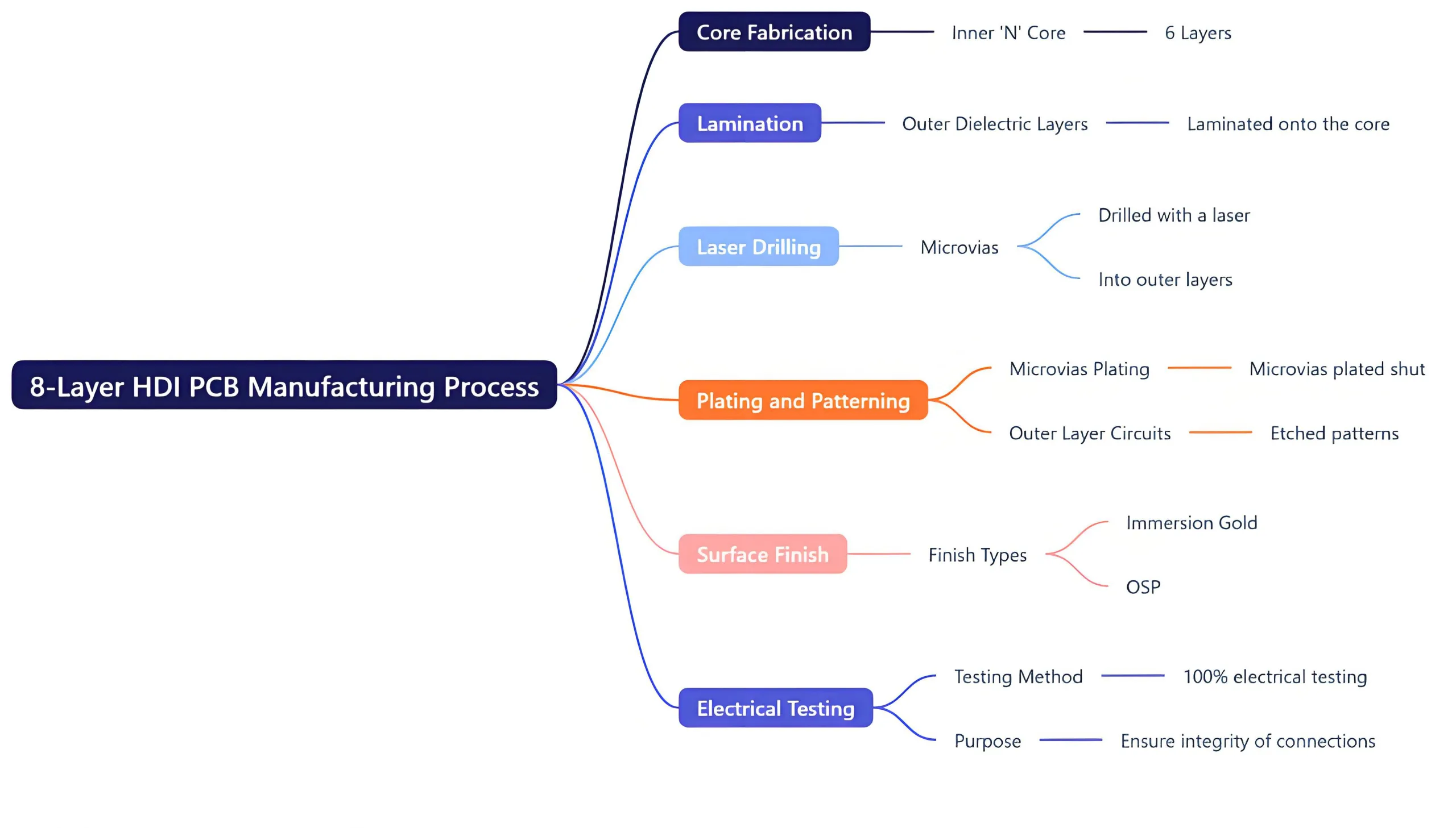
Производство этой печатной платы HDI представляет собой многоэтапный процесс., прецизионный процесс:
-
Изготовление ядра: Внутренний «Н»’ основной (6 слои) производится в первую очередь.
-
Ламинирование: Внешние диэлектрические слои наплавлены на сердечник..
-
Лазерное сверление: Микроотверстия просверливаются лазером во внешних слоях..
-
Покрытие и нанесение рисунка: Микроотверстия закрыты металлическими пластинами., и схемы внешнего слоя вытравлены.
-
Поверхностная отделка: Применяются Immersion Gold и OSP..
-
Электрические испытания: 100% электрические испытания гарантируют целостность всех соединений.
Почему стоит выбрать UGPCB для ваших потребностей в печатных платах HDI и PCBA?
Опыт UGPCB в производстве 8-слойных печатных плат HDI предлагает явные преимущества для вашего проекта.. Их способность надежно производить платы с 3/3 миллионные линии и микроотверстия 0,1 мм делают их лидером в производстве сложных печатных плат.. Это делает их идеальным партнером не только для Изготовление печатной платы но также и для полного обслуживания печатных плат «под ключ»., обеспечение плавного перехода от проекта к готовому продукту, собранный продукт.


