
Введение в 24 Плата объединительной платы для связи слоев
The 24 Печатная плата объединительной платы для связи между слоями представляет собой высокопроизводительную печатная плата предназначен для сложных систем связи. Он разработан для обеспечения надежного подключения и надежной передачи сигнала., что делает его идеальным для передовых телекоммуникационных приложений.
Что такое 24 Плата объединительной платы для связи слоев?
А 24 Плата объединительной платы связи слоев относится к многослойная печатная плата который был специально разработан с 24 слои проводящего материала, разделенные диэлектрическими слоями. Эта структура обеспечивает высокую плотность соединений, сохраняя при этом целостность сигнала и минимизируя помехи..
Требования к дизайну
Требования к проектированию 24 Уровни коммуникационной платы объединительной платы являются строгими из-за ее применения в критически важных системах связи.. Ключевые соображения дизайна включают:
- Материал: Panasonic M6, известен своими превосходными термическими и электрическими свойствами.
- Количество слоев: 24 уровни для удовлетворения сложных потребностей маршрутизации.
- Цвет: Синий/белый для легкой идентификации и эстетической привлекательности.
- Готовая толщина: 2.0мм, чтобы обеспечить структурную целостность и при этом не быть слишком громоздким..
- Толщина меди: 1OZ для обеспечения адекватной проводимости.
- Обработка поверхности: Погружение золота для повышения припая и коррозионной устойчивости.
Как это работает?
The 24 Коммуникация слоев. Плата объединительной платы работает с использованием нескольких слоев медных дорожек, разделенных диэлектрическими материалами.. Эти слои соединены между собой посредством металлизированных сквозных отверстий. (ПТХ) или переходные отверстия, позволяя сигналам перемещаться между разными слоями. Иммерсионная обработка поверхности золотом гарантирует, что медные дорожки остаются проводящими и устойчивыми к окислению..
Приложения
Основное применение средства 24 Уровни Коммуникационная плата объединительной платы находится в объединительных панелях связи, где решающее значение имеют высокоскоростная передача данных и надежное соединение.. Эти печатные платы используются в:
- Телекоммуникационная инфраструктура
- Центры обработки данных
- Устройства высокочастотной связи
- Сетевое оборудование
Классификация
На основе его функций и приложений, а 24 Плата объединительной платы уровней связи может быть классифицирована как печатная плата с высоким уровнем многослойности.. Эта классификация подчеркивает ее способность обрабатывать сложные и плотные схемы, необходимые для современных систем связи..
Материальная композиция
Ядро материал используется в 24 Плата объединительной платы связи слоев — Panasonic M6., высокопроизводительный ламинат материал, известный своим превосходным механическим, тепло, и электрические свойства. Этот материал гарантирует, что печатная плата выдержит требования приложений высокоскоростной связи..
Характеристики производительности
Эксплуатационные характеристики 24 Плата объединительной платы для связи слоев включает в себя:
- Высокая целостность сигнала
- Низкая потеря сигнала
- Превосходное тепловое управление
- Повышенная механическая прочность
- Надежная долгосрочная стабильность
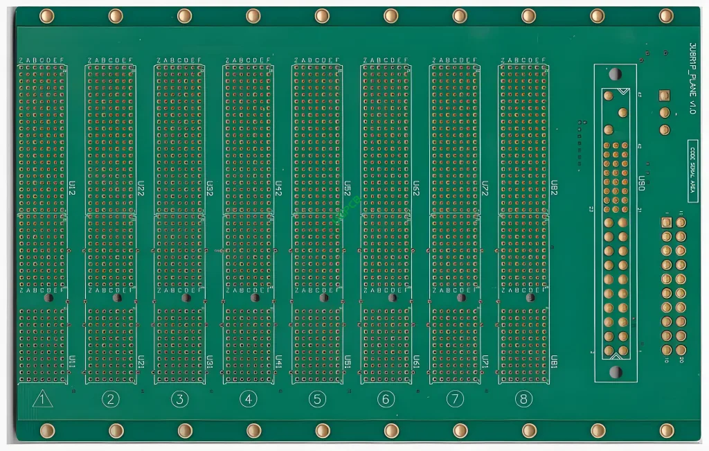
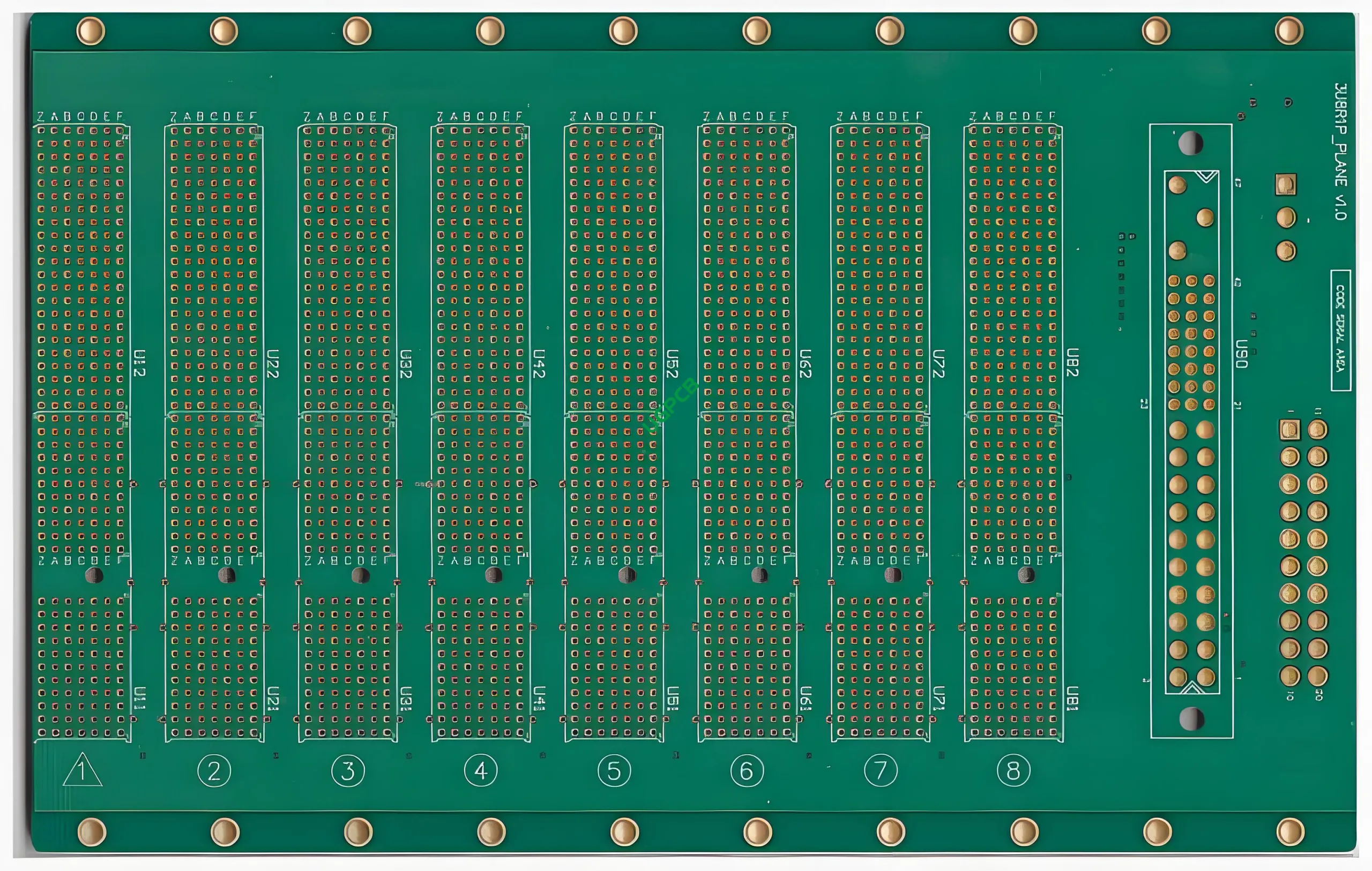
Структурные детали
Конструктивные детали 24 Уровни печатной платы объединительной платы связи следующие::
- Количество слоев: 24 слои
- Готовая толщина: 2.0мм
- Толщина меди: 1ОЗ
- Минимальная ширина трассировки: 6мил (0.15мм)
- Минимальное пространство между трассами: 6мил (0.15мм)
- Обработка поверхности: Погружение Золото
Функции и преимущества
Основные особенности и преимущества 24 Плата объединительной платы для связи слоев включает в себя:
- Взаимодействие высокой плотности
- Отличная целостность сигнала
- Надежная механическая конструкция
- Надежная долгосрочная производительность
- Эстетические варианты цвета (Синий/Белый)
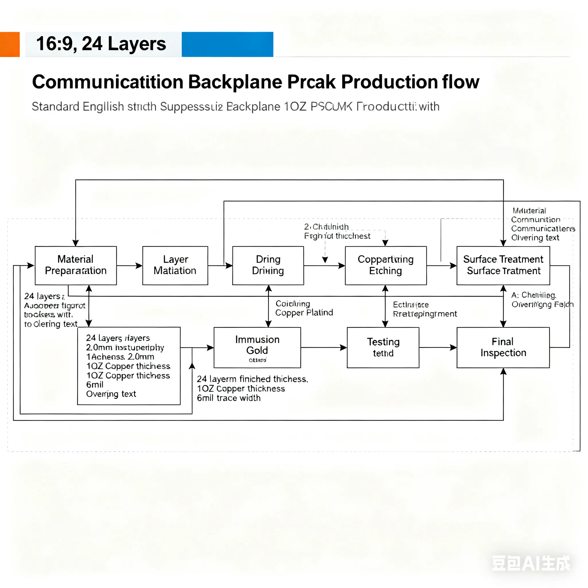
Производственный процесс
Производственный процесс 24 Коммуникация слоев. Плата объединительной платы включает в себя несколько этапов., включая:
- Выбор материала: Выбор качественного материала Panasonic M6.
- Наложение слоев: Аранжировка 24 слои с точностью.
- Офорт: Удаление лишней меди, чтобы сформировать желаемые схемы трассировки.
- Покрытие: Применение обработки поверхности погружения в погружение.
- Сборка: Включение PTH и VIAS для взаимосвязей слоя.
- Тестирование: Обеспечение печатной платы соответствует всем спецификациям производительности.
Варианты использования

The 24 Плата объединительной платы для связи слоев используется в различных сценариях., такой как:
- Высокоскоростные сети передачи данных
- Проекты телекоммуникационной инфраструктуры
- Передовое сетевое оборудование
- Приложения для центров обработки данных, требующие высокой пропускной способности
В итоге, а 24 Плата объединительной платы Layers Communication — это сложный и надежный компонент, разработанный для удовлетворения строгих требований современных систем связи.. Его дизайн высокой плотности, Отличные характеристики производительности, и прочная конструкция делают его неотъемлемой частью любой современной телекоммуникационной системы..


