
Engineered for High-Frequency RF Performance: The UGPCB 2-Layer Halogen-Free Antenna PCB Solution
In the era of IoT and high-speed wireless communication, antenna performance is paramount to device connectivity and stability. UGPCB’s 2-Layer Halogen-Free Antenna PCB is a high-performance, environmentally conscious printed circuit board solution engineered specifically for RF circuit design. It is more than a signal carrier; it is a critical component for optimizing antenna efficiency, ensuring precise impedance matching, and enhancing overall device reliability. With deep expertise in high-frequency дизайн печатной платы, we deliver a complete PCB to печатная плата solution through stringent process controls and meticulous material selection.
In-Depth Analysis: From Materials to Structure
1. Определение продукта
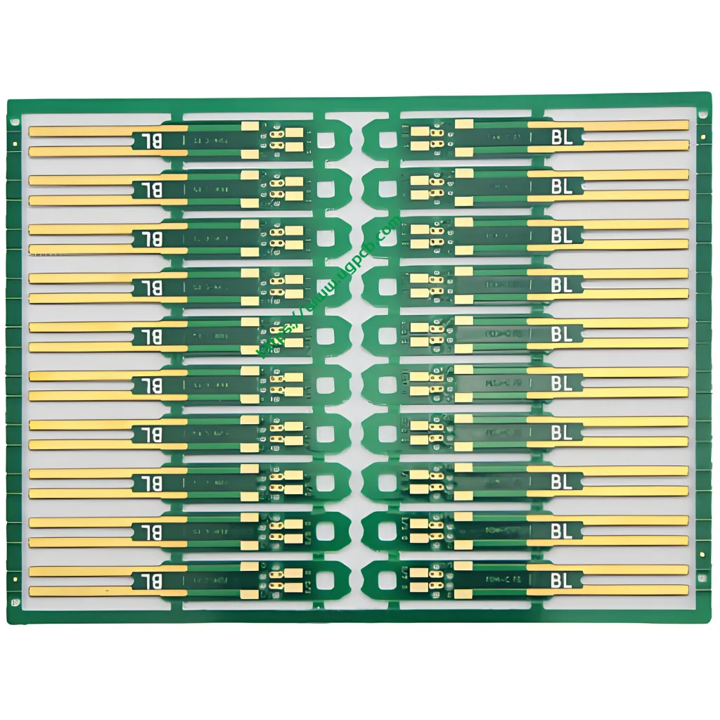
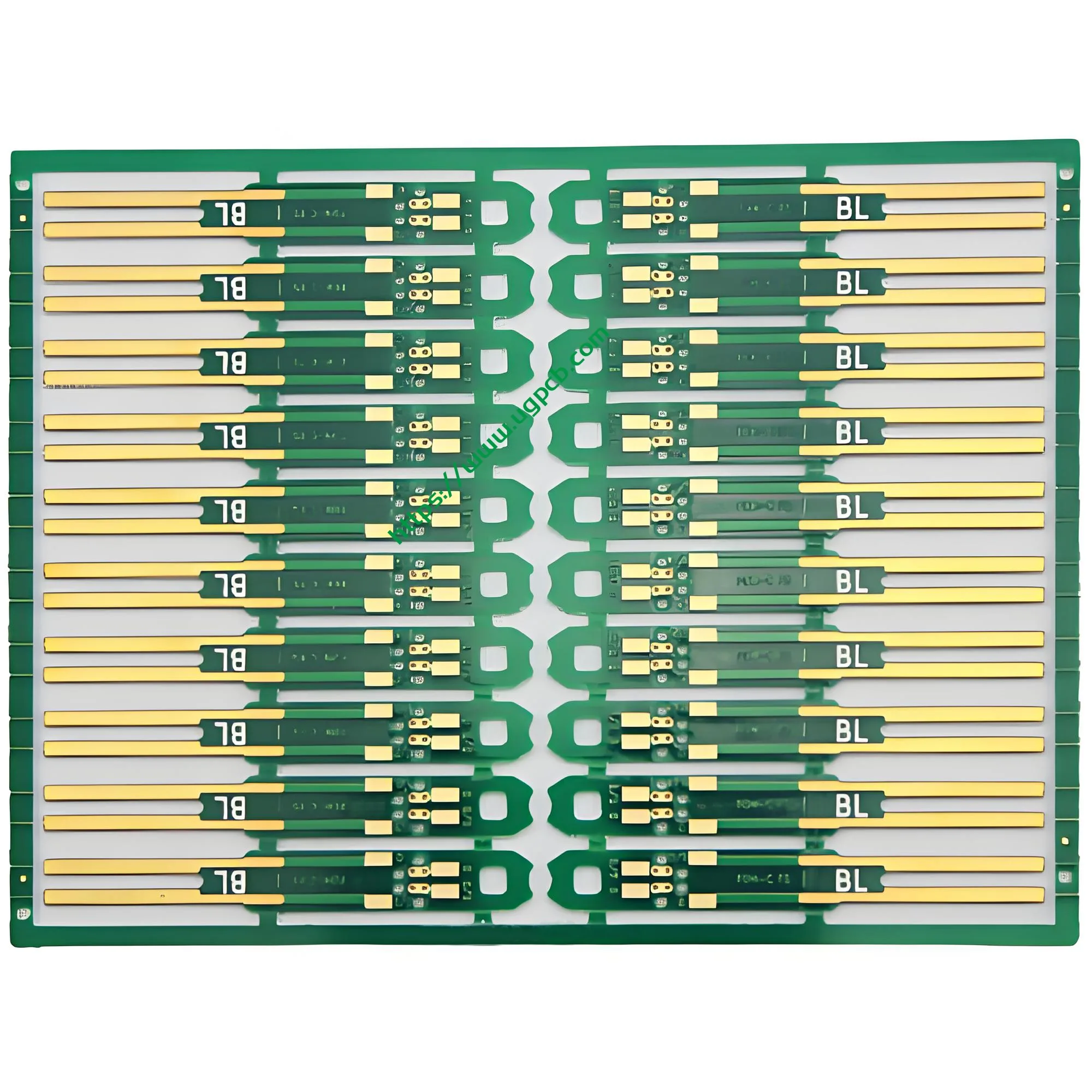
A 2-layer halogen-free antenna PCB is a double-sided circuit board dedicated to RF antenna circuitry. Its defining characteristic is the use of an environmentally friendly substrate free from halogens (хлор, бром). This makes it compliant with international directives like RoHS while meeting stringent RF performance requirements, making it particularly suitable for consumer electronics and export-oriented products.
2. Основные материалы & Электрические свойства
-
Материал подложки: Premium Halogen-Free FR-4 laminate. This material emits very low levels of toxic gases when combusted, offering enhanced safety and environmental benefits.
-
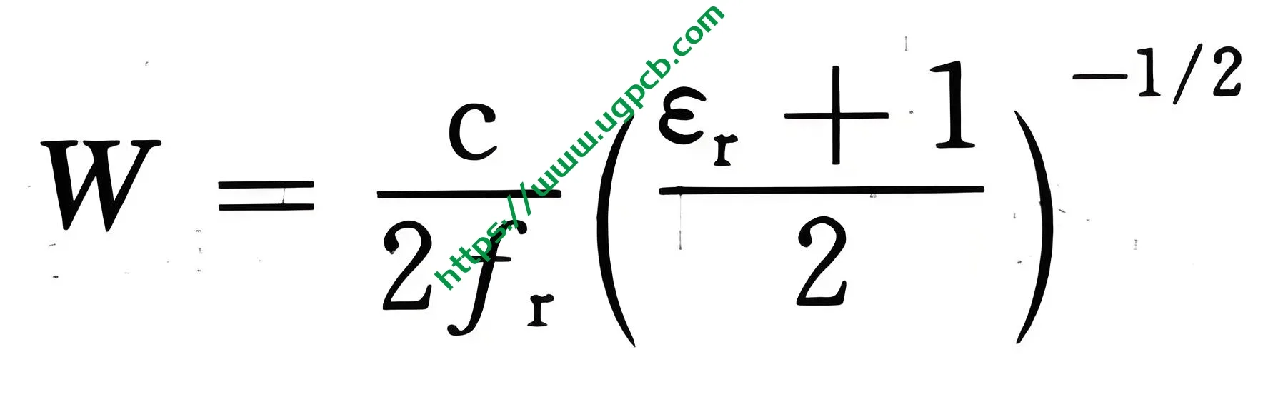
Диэлектрическая проницаемость (Дк): A stable Значение Dk 4.2. This is a critical parameter for antenna печатная плата дизайн. A stable Dk ensures consistent signal propagation velocity, forming the foundation for predictable antenna impedance control and performance.
-
Медный вес: Base copper of 0.5 ОЗ, finished copper thickness of 1 ОЗ (35мкм). The thickened copper layer helps reduce conductor loss and improves antenna radiation efficiency.
-
Поверхностная отделка: Погружение Золото (СОГЛАШАТЬСЯ). Provides excellent solderability, superior oxidation resistance, and a flat surface for antenna contact points or solder pads, making it ideal for the печатная плата and SMT assembly process.
3. Структурный дизайн & Ключевые параметры
-
Количество слоев & Толщина: 2-layer construction with a standard finished board thickness of 0.8mm, ideal for wireless modules and compact devices.
-
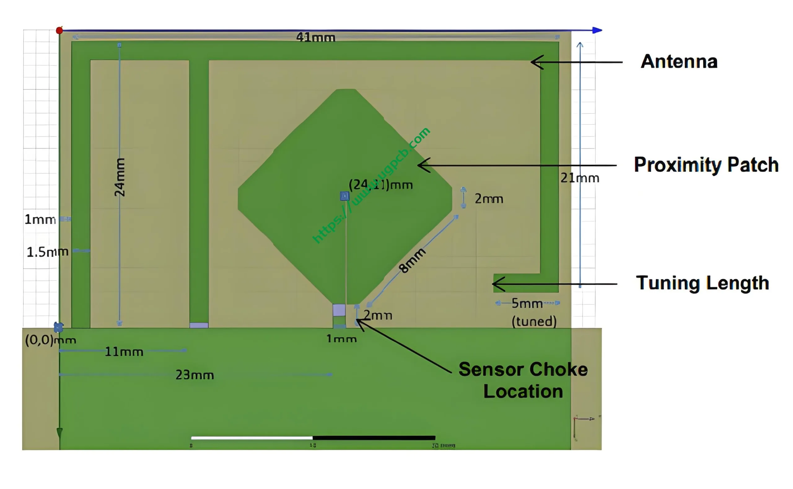
Line Precision: Minimum trace/space capability of 12mil/12mil. We maintain strict tolerances to ensure precise routing control, which is essential for accurate 50Ω microstrip transmission line design. This directly impacts antenna performance metrics like return loss and VSWR.
-
Solder Mask Options: Standard green or white solder mask. White mask is especially beneficial for laser marking and high-end product identification.
Основы дизайна & Принцип работы
Ключевые соображения по проектированию:
-
Сопоставление импеданса: Utilizing the stable Dk (4.2) and precise trace width control (12мил), designers can calculate or simulate exact 50Ω microstrip lines for perfect impedance matching between the antenna and the RF front-end.
-
Grounding Strategy: A well-planned ground plane (Гнездо) provides a complete return path for RF signals, minimizing interference and radiation loss.
-
Layout Isolation: Physically and spatially isolating the antenna section from other high-speed digital circuits (например, MCU, DC-DC преобразователи) to prevent noise coupling.
Принцип работы:
The copper traces on the antenna PCB are designed into specific geometries (например, Inverted-F Antenna, meander line antenna). When an RF signal travels from the chip through a matching network to the antenna, these traces convert the electrical signal into electromagnetic waves for radiation (transmit mode) or convert incoming electromagnetic waves into electrical signals (receive mode). The efficiency of this process is highly dependent on the dielectric stability of the PCB laminate and the precision of the trace fabrication.
Функции & Преимущества
-
Stable High-Frequency RF Performance: Consistent Dk (4.2) and strict trace tolerances ensure reliable, repeatable antenna performance across production batches.
-
Eco-Friendly & Надежный: Halogen-free materials meet green manufacturing standards, enhancing product safety and market accessibility.
-
High-Process Quality: ENIG surface finish offers oxidation resistance and long shelf life, providing perfect pads for subsequent SMT assembly and PCBA процессы.
-
Expert Design Support: UGPCB offers Обзор конструкции печатной платы services to help customers optimize antenna layout and stack-up, avoiding common RF design pitfalls.
-
Предложение изображения 2: Microscope image comparing precise 12mil trace/space edges.
-
Изображение Alt Text: Close-up of high-precision 12mil trace/space on PCB, critical for consistent antenna impedance.
Производственный процесс & Гарантия качества
UGPCB’s production workflow strictly adheres to the special requirements for high-frequency Производство печатных плат:
Engineering Review → Halogen-Free Material Cutting → Laser Drilling → Deposition & Plating → Precision Pattern Transfer → Acid Etching (Strict Line Width Control) → ENIG Surface Finish → Solder Mask Application → Electrical & Flying Probe Testing → Final Inspection & Упаковка.
We implement enhanced controls, particularly during pattern transfer and etching, to achieve stringent trace tolerance requirements. Stability of the Dk value is verified through periodic sampling with network analyzers.
Широкий спектр применения
This 2-layer halogen-free antenna PCB serves as the “heart” of numerous wireless communication devices. Typical applications include:
-
IoT устройства: Smart home sensors, Bluetooth modules, LoRa modules.
-
Network Communications: Wi-Fi маршрутизаторы, wireless access points, network cameras.
-
Бытовая электроника: Wireless headphones, remote controls, wearable technology.
-
Промышленный контроль: Wireless data collectors, remote monitoring terminals.

Whether you require rapid prototype Изготовление печатной платы or large-scale volume production, UGPCB provides reliable, эффективный antenna PCB manufacturing and comprehensive Услуги по сборке печатных плат to accelerate your product’s time-to-market.
-
Предложение изображения 3: Collage of application scenarios (PCB integrated into end-products like smart home devices, маршрутизаторы, носимые устройства).
-
Изображение Alt Text: Application of 2-layer halogen-free antenna PCB in Wi-Fi routers, IoT sensors, and wireless devices.
Contact us today to get your customized 2-Layer Halogen-Free Antenna PCB solution and quote! Let UGPCB’s expertise become the solid foundation for your wireless product’s success.


