Overview of the 8L 8L 2+N+2 HDI PCB Product
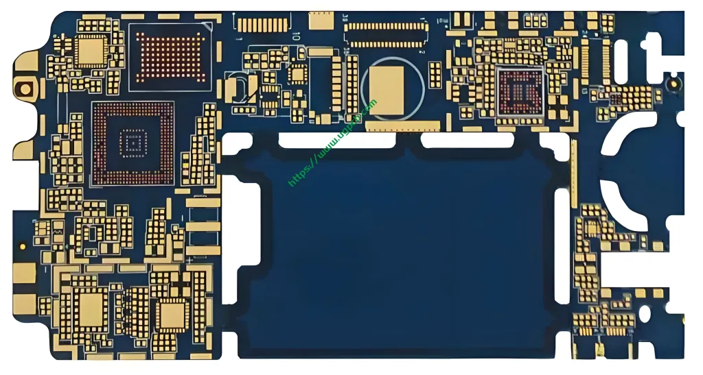
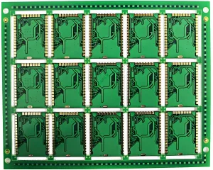
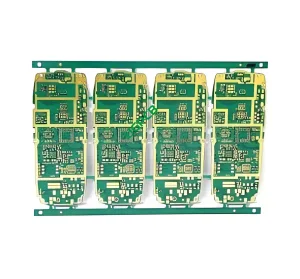
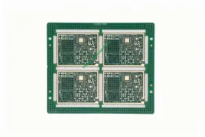
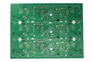
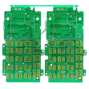
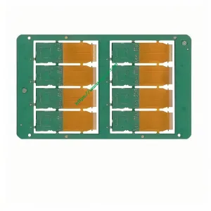
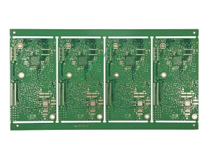
The 8L 8L 2+N+2 HDI PCB product is a high-density interconnect printed circuit board designed for advanced electronic applications. It features a complex structure with multiple layers and specialized processes to meet the demands of modern intelligent digital products.
Definition and Design Requirements
The 8L 8L 2+N+2 HDI PCB stands for a printed circuit board with eight layers on each side, two power layers, N signal layers, and two additional signal layers. The design requirements include high density, precise trace and space measurements, and specific hole sizes for mechanical and laser drilling.
Принцип работы
The HDI PCB works by providing intricate electrical connections between various components on the board. The high-density layout allows for more components to be packed into a smaller space, improving overall functionality and performance.
Приложения
These PCBs are primarily used in intelligent digital products where compact size, высокая производительность, and reliability are crucial. They are ideal for applications such as smartphones, таблетки, and other portable electronic devices.
Классификация
HDI PCBs can be classified based on their layer count, материал, and special processes. The 8L 8L 2+N+2 configuration indicates a specific type of multilayer PCB with enhanced capabilities.
Материал
The primary material used for this PCB is FR-4, which is a flame-resistant glass-epoxy laminate. Этот материал обеспечивает превосходную тепловую стабильность, механическая прочность, and electrical insulation properties.
Производительность
The 8L 8L 2+N+2 HDI PCB offers superior electrical performance, including low signal loss and high-speed data transmission. Its immersion gold and OSP surface treatments ensure long-lasting durability and reliable connections.
Структура
The structure of this PCB includes eight layers on each side, with internal and external copper thicknesses of 1OZ and 0.5OZ, соответственно. The finished thickness of the board is 1.0mm, and it features blind holes for increased connectivity.
Функции
Key features of this PCB include:
- High-density interconnect design
- Precision trace and space measurements (3мил/3мил)
- Mechanical holes of 0.2mm and laser holes of 0.1mm
- Specialized surface treatments for enhanced durability
Производственный процесс
The production process for an 8L 8L 2+N+2 HDI PCB involves several steps, включая:
- Material preparation and layer stacking
- Drilling of mechanical and laser holes
- Copper plating and etching
- Surface treatment application
- Final inspection and testing
Each step is carefully executed to ensure the highest quality and performance of the final product.
Варианты использования
This PCB is commonly used in:
- Smartphones and tablets
- Wearable technology
- High-density computing systems
- Advanced communication devices
В заключение, the 8L 8L 2+N+2 HDI PCB product is a state-of-the-art solution for modern intelligent digital products, offering unparalleled performance, надежность, and compactness.
 ЛОГОТИП УГКПБ

