
The rapid growth of 5G, промышленная автоматизация, and medical electronics demands higher reliability, integration, and spatial adaptability from circuit boards. Жесткая пласка (R-FPCB) combines the mechanical stability of rigid PCBs with the bending adaptability of flexible PCBs, making it a core technology for high-end electronic designs. According to DIResearch, the global rigid-flex PCB market reached $2.604 миллиард в 2025 и, по прогнозам, вырастет до $3.726 миллиард за 2032, в Cagr 5.25%. UGPCB follows this trend with advanced equipment and strict quality control, offering the 6-layer panel button Rigid-Flex PCB – a high-performance, high-reliability solution for industrial equipment.
1. What Is a 6-Layer Rigid-Flex PCB? – Definition and IPC Standards
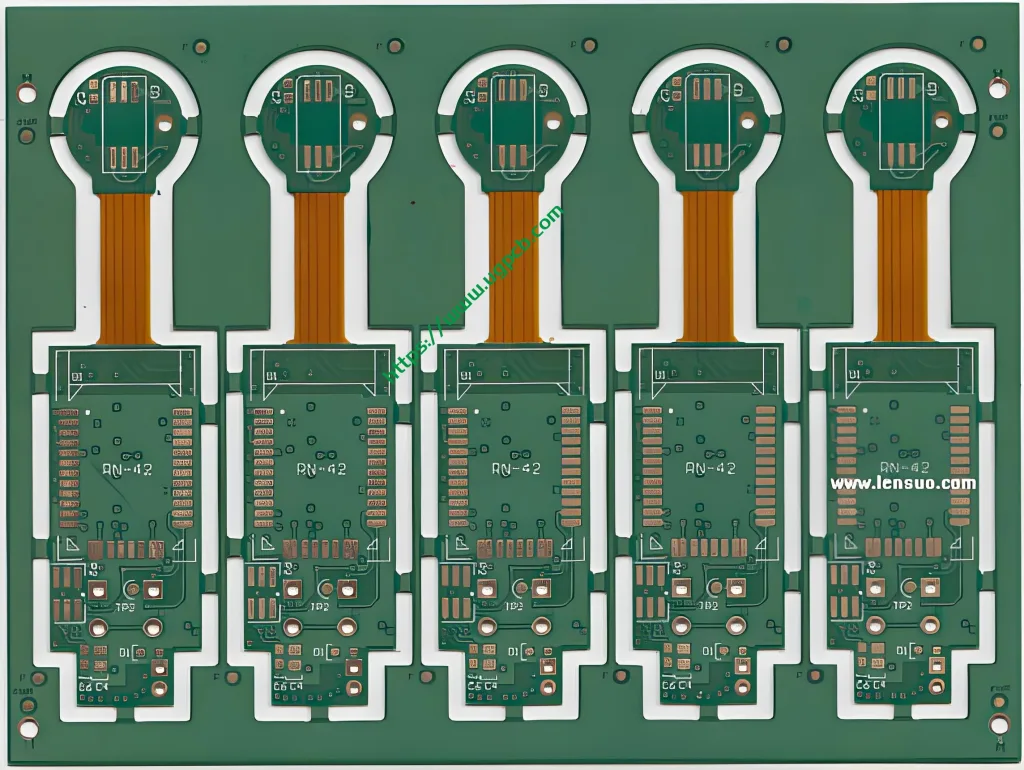
A rigid-flex PCB combines rigid and flexible circuit boards into one interconnect structure using lamination. Its key feature: a single board has both rigid areas (для монтажа компонентов) and flexible areas (for bending and 3D layout). According to IPC-6013D, rigid-flex PCBs fall into five types. Тип 4 – multilayer rigid and flexible materials with three or more conductive layers and PTH – matches this product. UGPCB’s 6-layer rigid-flex PCB uses a hybrid structure: 4 FR4 rigid layers + 2 полиимид (ПИ) flexible layers, enabling high-density routing in rigid areas and dynamic/static bending in flexible areas.
This product follows IPC-2221 design guidelines and meets Сорт 2/3 performance levels, suitable for industrial equipment, medical instruments, and automotive electronics that demand high reliability.
2. Key Technical Parameters – The Strength of a High-Performance Rigid-Flex PCB
UGPCB verifies all core parameters of its 6-layer button panel rigid-flex PCB through strict process control, complying with IPC-6012 and IPC-4562 standards.
| Параметр | Спецификация |
|---|---|
| Модель | 6-layer panel button Rigid-Flex PCB |
| Стек-ап | 4 FR4 rigid layers + 2 PI flexible layers |
| Законченная толщина | 0.15 мм |
| Медная толщина фольга | 1 унция (nominal 35 мкм) |
| Спорная маска цвет | Зеленый / Белый |
| Чистота поверхности | СОГЛАШАТЬСЯ (Химическое никель, иммерсионное золото) |
| Мин. след/пространство | 6 мил / 6 мил (0.1524 мм) |
| Мин. mechanical drill | 0.2 мм |
| Приложение | Industrial equipment circuit boards |
Copper thickness note: 1 oz copper foil has a nominal thickness of 35 мкм (exactly 34.798 мкм). Per IPC-4562, the tolerance is ±10%, so the actual thickness must range from 31.31 µm to 38.5 мкм. This ensures current-carrying capacity and impedance consistency for the rigid-flex PCB.
Reliability of 6 Мил трасса/пространство: IPC-2221 recommends a minimum electrical clearance of 0.1 мм (~4 mil) for low-voltage applications (<15В). Наш 6 мил (0.1524 мм) design exceeds this baseline, providing ample signal isolation margin in complex industrial electromagnetic environments, reducing crosstalk and electrical noise.
3. Design Considerations for Rigid-Flex PCBs
Designing a rigid-flex PCB requires balancing rigid and flexible areas. The transition zone between them is critical for long-term reliability. Here are the key design points UGPCB focuses on:
3.1 Rigid-Flex Transition Zone Design
IPC-6013 defines the transition zone as a 3 mm region centered on the rigid board edge. This area experiences high stress and is prone to cracks, расслаивание, and copper fatigue. UGPCB avoids placing any functional features (vias, подушечки, critical traces) in this zone. We also use no-flow or low-flow prepreg sheets to prevent resin from flowing into the flexible area.
3.2 Bend Radius and Dynamic Fatigue Life
Bending performance depends on material thickness and bend radius. The empirical formula is:
-
Dynamic bending minimum radius ≥ 10 × total flexible area thickness
-
Static bending (one-time installation) минимальный радиус ≥ 6 × total flexible area thickness
With an ultra-thin total thickness of 0.15 мм, this product achieves stable bending at radii as small as 1.5 мм, suiting complex routing paths in industrial equipment. UGPCB’s flexible area withstands over 100,000 циклы гибки, and for high-dynamic applications it can reach 500,000 цикл (R=5 mm, 180°往复 bending).
3.3 Copper Thickness and Flexible Area Traces
Thick copper in the flexible area reduces flexibility and increases fatigue risk. Поэтому, UGPCB uses an optimized copper thickness strategy: the rigid layers maintain 1 oz for sufficient current, while the flexible layers use thinner copper adapted for bending. A cross-hatched copper pattern in the flexible area effectively reduces stress concentration from solid copper, improving dynamic bending life.
4. Working Principle of Rigid-Flex PCBs
The working principle of a rigid-flex PCB is based on integrated interconnect design. Rigid areas provide stable mechanical support and heat dissipation for components (чипсы, резисторы, конденсаторы, разъемы). Flexible areas handle signal connection and bending between rigid areas. Conductive patterns on each layer connect electrically through plated through holes (ПТХ). During installation or operation, the flexible area bends, folds, or dynamically flexes according to the mechanical structure, while components and solder joints in rigid areas remain fixed and stress-free.
This design eliminates the traditional combination of rigid board + flexible cable + разъемы, thus reducing solder joints, lowering signal reflection and impedance mismatch risks, and significantly improving vibration and shock resistance.
5. Classification of Rigid-Flex PCBs (IPC-6013D)
| IPC Type | Определение | Проводящие слои | Функции |
|---|---|---|---|
| Тип 1 | Single-sided flexible PCB | 1 | With or without stiffener |
| Тип 2 | Double-sided flexible PCB | 2 | With PTH |
| Тип 3 | Multilayer flexible PCB | ≥3 | With PTH |
| Тип 4 | Multilayer rigid-flex combination | ≥3 | Жесткий + flexible materials, with PTH – our product |
| Тип 5 | Flexible/rigid-flex PCB | ≥2 | Without PTH |
For installation use, this product applies to Use A (bend once for installation) и Use B (continuous dynamic bending).
6. Materials and Performance Advantages
6.1 FR4 Rigid Layer
ФР4 (Flame Retardant 4) is the most mature substrate for rigid PCBs. It offers excellent mechanical strength, good dielectric properties, и огнестойкость, making it widely used in industrial equipment. FR4’s glass transition temperature (Тг) typically ranges from 130°C to 170°C, ensuring dimensional stability in high-temperature industrial environments.
6.2 Полиимид (ПИ) Flexible Layer
Polyimide is the mainstream substrate for flexible PCBs. It provides high temperature resistance (operating range -55°C to +150°C), good dielectric strength, and excellent chemical resistance. PI has a dielectric constant (Дк) of about 3.4–3.5 and a dissipation factor (Дф) of about 0.002–0.008, making it suitable for high-speed signal transmission. UGPCB uses an adhesiveless polyimide laminate in the flexible area. Compared to traditional adhesive-based laminates, adhesiveless structures are thinner (by 12–25 µm), achieve smaller bend radii (вплоть до 1 мм), and have more stable Z-axis expansion, significantly improving reliability under dynamic bending.
6.3 ENIG Surface Finish
СОГЛАШАТЬСЯ (Химическое никель, иммерсионное золото) is a two-metal layer finish: a nickel layer (приблизительно. 3–6 µm thick) and a gold layer (приблизительно. 0.05–0.1 µm thick). The gold layer provides excellent oxidation resistance and solderability. The nickel layer acts as a barrier preventing copper diffusion into gold. ENIG is especially suitable for button panels, gold finger connectors, and high-reliability pads, ensuring stable contact performance after repeated plugging and long-term use.
7. Функции производительности
UGPCB’s 6-layer rigid-flex PCB offers these core advantages:
-
Space saving: Rigid-flex integration eliminates connectors and cables, saving 30–50% of installation space compared to traditional “rigid board + cable” solutions.
-
Weight reduction: Polyimide has low density (приблизительно. 1.42 G/CM³), significantly lowering overall structural weight.
-
Improved reliability: Eliminating solder joints and mechanical connectors reduces failure rates. Studies show that rigid-flex PCBs cut failure rates in vibration environments by about 70%.
-
Целостность сигнала: Continuous routing avoids impedance discontinuities at connectors, benefiting high-frequency signal transmission.
-
Vibration and shock resistance: The flexible area acts as a natural buffer, absorbing mechanical vibrations and protecting components in rigid areas.
-
3D assembly capability: The board adapts to complex spatial layouts, folding and bending to fit irregular enclosure shapes.
8. Manufacturing Process for Rigid-Flex PCBs
UGPCB follows IPC-6013 and IPC-6012 standards in its rigid-flex PCB production process:
-
Flexible substrate cutting – Cut PI copper-clad laminate to size.
-
Inner layer circuit formation – Create inner layer circuits on flexible and rigid layers (контакт, разработка, травление).
-
AOI Inspection – 100% automated optical inspection for opens/shorts.
-
Ламинирование – Laminate FR4 rigid layers and PI flexible layers using low-flow prepreg under high temperature and pressure, with spacers to prevent resin from flowing into flexible areas.
-
Бурение – Mechanical drilling (мин. 0.2 мм) и лазерное бурение (для микроотверстий).
-
PTH and plating – Deposit copper in holes and plate to specified thickness.
-
Outer layer circuit formation – Transfer and etch outer layer patterns.
-
Solder mask coating – Apply green or white solder mask ink, selectively opening pads.
-
Чистота поверхности – ENIG treatment.
-
Маршрутизация – Mill the outline, cut away rigid material covering flexible areas to expose the flex section.
-
Электрическое испытание – Flying probe or fixture test to ensure continuity.
-
FQC and shipping – Final quality inspection followed by vacuum packaging.
This process ensures reliable bonding between FR4 rigid areas and PI flexible areas, while PTH hole wall copper thickness meets IPC-6012 Class 2/3 требования (minimum 18–20 µm).
9. Classification by Structure and Application
| Классификация | Subtype | Описание |
|---|---|---|
| Количество слоев | 2 / 4 / 6 / 8+ слои | Этот продукт: 6 слои (4R+2F) |
| Rigid-flex layout | Symmetrical / Asymmetrical | Asymmetrical: flexible layers on one side of rigid layers |
| Bend type | Статический / Динамика | Статический: one-time installation; Динамика: repeated bending |
| Via type | Full PTH / Blind/buried / ИЧР | Этот продукт: full PTH |
| Solder mask process | Coverlay / Припаяная маска чернила | Coverlay is better for flexible areas |
Этот продукт представляет собой multilayer symmetrical rigid-flex PCB (Тип 4) with a rigid-to-flex layer ratio of 4:2, full PTH structure, solder mask ink on rigid areas, and coverlay protection on flexible areas.
10. Main Use Cases – Industrial Equipment Applications
UGPCB’s 6-layer rigid-flex PCB is designed specifically for industrial equipment. Typical applications include:
-
Industrial control panels and button systems – Button panels need rigid areas (button contacts) and flexible areas (signal routing) in one board. Rigid-flex PCBs perfectly meet this need while eliminating connector solder joints, greatly improving panel mechanical reliability.
-
Automation equipment and robots – Signal transmission in robotic joints undergoes continuous bending. The dynamic bending capability of rigid-flex PCBs supports high-cycle requirements.
-
Test and measurement instruments – Compact test devices benefit from 3D routing, optimizing space utilization.
-
Industrial sensor modules – Flexible areas conform to device housings or curved surfaces, enabling seamless connection between sensors and main control boards.
-
Industrial display modules – Interconnection between LCD/LED displays and driver boards is simplified with rigid-flex PCBs, reducing thickness and improving vibration resistance.
-
Медицинские приборы – Portable ultrasound units, patient monitors, and other medical instruments demand miniaturization, легкий вес, and high reliability – rigid-flex PCBs are an ideal choice.
-
Автомобильная электроника – In-vehicle control units and sensor modules require vibration resistance and high-temperature tolerance.
Rigid-flex PCBs excel in three capability dimensions: dynamic bending, high-vibration environments, and compact spaces – especially suitable for demanding industrial equipment applications.
11. Why Choose UGPCB Rigid-Flex PCBs?
UGPCB combines years of PCB manufacturing experience with advanced automated production lines to provide a one-stop rigid-flex PCB solution for global customers:
-
Layer count support: 4 к 24 layers of rigid-flex combination, supporting HDI high-density interconnect designs.
-
Ultra-fine circuits: Minimum trace/space down to 1.5 mil/1.5 mil with tolerance within ±5%.
-
High-precision impedance control: Impedance tolerance as tight as ±5%, suitable for high-frequency applications above 10 ГГц.
-
Total quality management: The factory implements TQM with 100% AOI Inspection + AI defect prediction, achieving a yield rate above 98%.
-
One-stop service: From PCB design and manufacturing to PCBA assembly and component sourcing, UGPCB offers a complete industrial chain service, shortening R&D cycles and accelerating product launch.
Get a Quote & Technical Support for UGPCB’s 6-Layer Rigid-Flex PCB
UGPCB provides:
-
Real-time online support system – 7×24 hour professional technical assistance.
-
Free DFM check – Professional design-for-manufacturability review to avoid design flaws.
-
Fast prototyping and volume production – Sample lead time: 7–10 working days; volume production: 2–3 weeks.
-
Global logistics – Support for DHL, FedEx, UPS, and other international couriers.
Visit the UGPCB official website to submit your rigid-flex PCB inquiry, or contact the UGPCB technical team for a customized 6-layer button panel rigid-flex PCB solution.
*Data sources: IPC-6013D standard parameters, IPC-2221 electrical clearance guidelines, and IPC-4562 copper foil tolerance data are based on authoritative industry standards. Global market size data comes from DIResearch and QYResearch public reports.*


