
Communications PCBs Applications
Communications PCBs are also used in general telecommunications systems such as cell towers, спутники, high-speed routers and servers, and commercial telephony. Telecom PCBs are also frequently used to control LED displays and indicators.
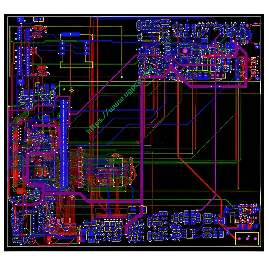
Structure and Composition of High-Frequency Hybrid Splint
Base Plate and Wire Layers
The high-frequency hybrid splint includes a base plate, which is folded and positioned on the first inner wire layer, the first outer wire layer, and the top surface of the solder mask ink layer from top to bottom in order from bottom to top.
Solder Resist Ink Layer and Substrate Areas
The second layer of solder resist ink layer, the substrate includes a high-frequency area and an auxiliary area. The auxiliary area is finally fixed, and the inlay in the high-frequency area should be located at a fixed position.
Functionality and Material Usage
Utility Model Description
The utility model provides a high-frequency hybrid splint, which is divided into two parts: a high-frequency area and an auxiliary area. It provides mechanical support.
High-Frequency Area Arrangement
The utility model discloses that the high-frequency area is independently arranged, and only the high-frequency area is made of high-frequency materials. Under the condition of satisfying high-frequency signals, the use of high-frequency board materials is minimized and the production cost is reduced.


