
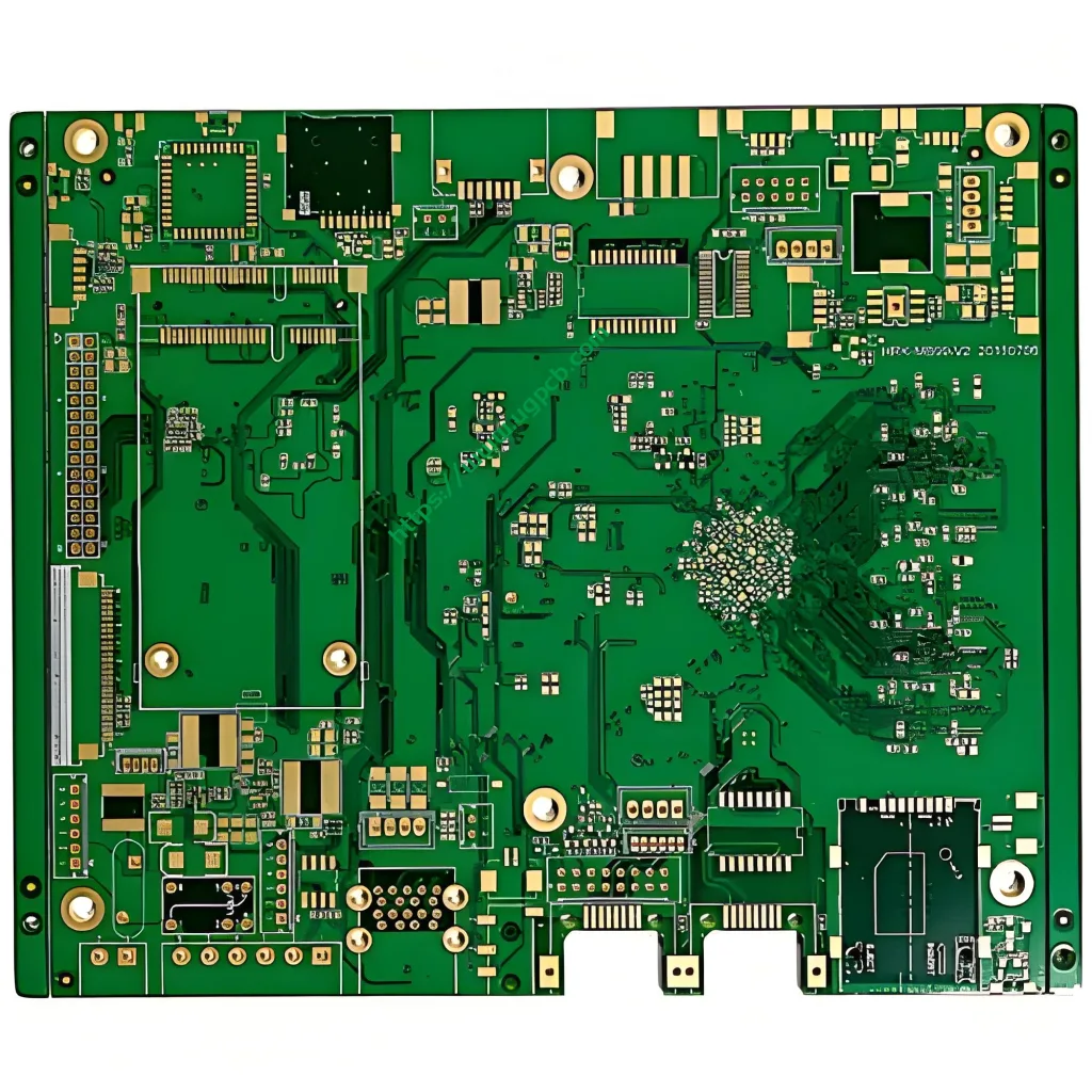

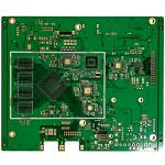
What is an 8-Layer PCB?
An 8-layer PCB is a multilayer PCB that provides ample routing space for applications that require multiple power islands. This printed circuit board can help improve EMC performance by adding two planes.
Usage of 8-Layer PCB
The board is usually mounted on compact devices such as motherboards, wearable watches, backplanes, и т. д.. The increased cost of the 8-layer PCB justifies the increased cost for excellent EMC performance. An 8-layer PCB stackup consists of 4 planes and 4 routing layers connected by 7 rows of dielectric material.
Structure of 8-Layer PCB
The PCB uses a six-layer board with higher EMC performance. 8-слойная печатная плата запечатана с приподкой маской на дне и вверху.
Преимущества 8-слойного стека PCB-Up-Up
У 8-слойного стека PCB есть множество преимуществ, которые делают его идеальной заменой для других материалов для платы. Ниже приведены преимущества этих печатных плат:
Минимизировать хрупкость
8-Пчела слоя снижает хрупкость устройства, Улучшение общей производительности. Это помогает защитить внутренний слой от шума, тем самым снижая его уязвимость для внешних сил.
Снижение радиации
Этот тип многослойного стека помогает устранить любое излучение, которое может произойти в высокоскоростных приложениях. В отличие от других стеков, 8-слойная печатная плата устраняет излучение EMI.
Снижение эксплуатационных расходов
8-Стоки платы слоя является экономически эффективным вариантом. Что касается замены и очистки, Этот стек может сэкономить вам много денег. This means that the 8-layer PCB stackup requires low maintenance and is very durable.
Increased Functionality
Choosing an 8-layer PCB will help increase the speed and functionality of the device used. Such printed circuit boards are more reliable and practical in different applications. This PCB has more than 4 layers of conductive material to enhance the signal traces.
Application of 8-Layer PCB Stackup
The 8-layer PCB stackup is the most common type of stackup found in most appliances. This multilayer PCB can be useful in a variety of applications such as:
- Medical industry
- Automotive industry
- Manufacturing
- Chemical processing industry
- Aviation Industry


