Материальная композиция
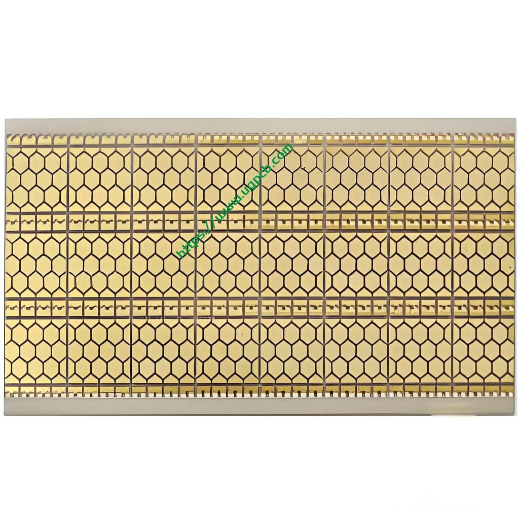
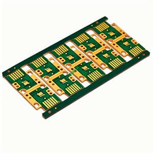
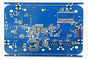
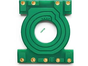
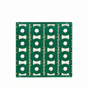
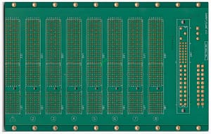
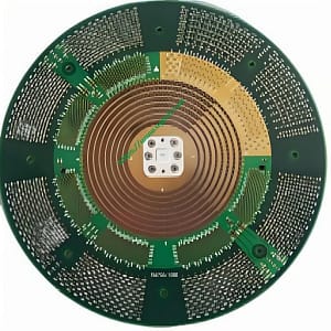
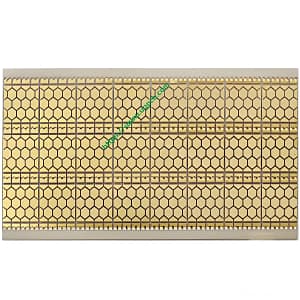
The Aluminum Nitride Ceramic PCB is composed of high-quality ceramic materials, specifically ceramic PCB and ceramic substrate. This combination ensures exceptional thermal conductivity and electrical insulation properties.
Характеристики производительности
The печатная плата features a 2-layer ceramic structure with a white color appearance. The thickness of the aluminum nitride layer is precisely 0.635mm, обеспечивая прочную основу для компоненты. Толщина меди 1 унция (35один) ensures good electrical conductivity, while the immersion gold surface treatment with a gold thickness of >= 3U” enhances corrosion resistance and ensures smooth soldering processes.
Отличительные особенности
- Высокая теплопроводность: Aluminum nitride offers excellent thermal conductivity, making it suitable for high-power and high-frequency applications.
- Долговечность: Ceramic materials are known for their hardness and durability, contributing to the PCB’s long lifespan.
- Точность: The minimum aperture of 0.8mm allows for the placement of fine components, ensuring high-density packaging.
Производственный процесс
The production of Aluminum Nitride Ceramic PCBs involves several critical steps:
- Подготовка материала: High-quality aluminum nitride powder and other ceramic materials are mixed and pressed into the desired shape.
- Sintering: The pressed ceramic substrate undergoes sintering at high temperatures to achieve the required density and strength.
- Отложение меди: A layer of copper is deposited on the ceramic substrate using advanced metallization techniques.
- Паттерн схемы: Медный слой травится для формирования желаемого рисунка схемы..
- Hole Drilling: Through holes are drilled to allow for interconnections between layers.
- Ceramic Dam Technology: This unique technology ensures the precise alignment and sealing of holes, enhancing the PCB’s reliability.
- Обработка поверхности: The PCB undergoes immersion gold plating to provide a corrosion-resistant surface finish.
Сценарии приложения
Aluminum Nitride Ceramic PCBs are ideal for various high-performance applications:
- High-Power Electronics: Suitable for use in power supplies, inverters, and other high-power electronic devices due to their excellent thermal management capabilities.
- Высокочастотные схемы: Perfect for RF and microwave circuits that require low loss and high stability.
- Медицинское оборудование: Used in medical devices that demand precision, надежность, and high-performance electronics.
- Аэрокосмическая и защита: Ideal for applications in harsh environments where durability and thermal resistance are crucial.

В итоге, Aluminum Nitride Ceramic PCBs offer a combination of exceptional thermal conductivity, долговечность, and precision, making them ideal for high-performance electronics across various industries.
 ЛОГОТИП УГКПБ

