
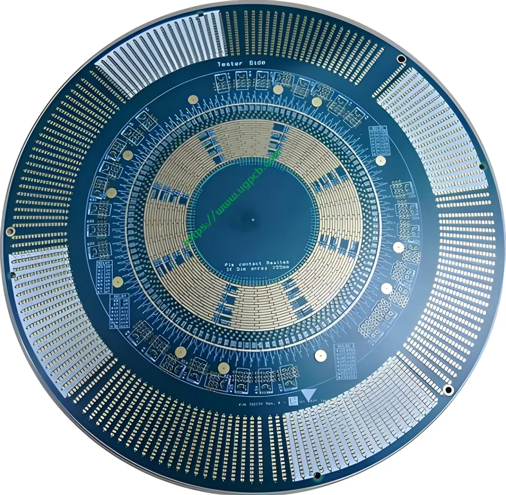
ATE Test Chip PCB Overview
The ATE test chip PCB is a specialized printed circuit board designed for use in automated test equipment (ЕЛ) systems for testing semiconductor chips. This PCB plays a crucial role in ensuring the quality and reliability of chips before they are integrated into electronic devices. Below is a detailed introduction to the ATE test chip PCB, охватывая свою общую информацию, классификация, материалы, производительность, структура, функции, производственный процесс, и сценарии приложений.
Классификация
ATE test chip PCBs are classified based on their layer count, material composition, и конкретные требования к применению. Модель представлена здесь, ATE test chip PCB, is a 12-layer PCB, indicating its complexity and ability to handle intricate testing scenarios.
Материальная композиция
The ATE test chip PCB is constructed using isola 370hr material, a high-performance, high-reliability substrate known for its excellent electrical and thermal properties. This material ensures the PCB’s ability to withstand the demanding test conditions and provide stable performance.
Характеристики производительности
The ATE test chip PCB excels in several performance areas, в том числе высокая пропускная способность переноса, низкая потеря сигнала, и отличное тепловое управление. The use of 2OZ copper thickness for inner layers and 1OZ for outer layers enhances its electrical conductivity and thermal dissipation capabilities. Кроме того, the immersion gold (5U) surface finish provides superior corrosion resistance and solderability, ensuring reliable connections during testing.
Структурный дизайн
Структурно, the ATE test chip PCB features a board thickness of 3.0mm, Обеспечение надежной основы для сложной схемы и компонентов. The green color not only adds a visual distinction but also aids in inspection and troubleshooting processes.
Отличительные особенности
The ATE test chip PCB stands out with its unique features, including its high layer count, advanced material composition, and immersion gold surface finish. Эти функции, combined with its precise design and manufacturing processes, make it an ideal choice for ATE chip testing applications.
Производственный процесс
The production of ATE test chip PCBs involves a series of sophisticated steps:
- Подготовка материала: The isola 370hr substrate is prepared and cut to the required dimensions.
- Медная ламинирование: Медная фольга ламинирована на подложке, with specific attention to the inner layer 2OZ and outer layer 1OZ thickness requirements.
- Паттерн схемы: Желаемые схемы схемы выгравируются на медной фольге с использованием методов точности травления.
- Укладка слоя и ламинирование: Несколько слоев сложены и ламинируются вместе, обеспечение точного выравнивания и соединения.
- Сверление и покрытие: Holes are drilled for component mounting and interconnection, and then plated to enhance conductivity.
- Применение поверхности: The immersion gold (5U) coating is applied to provide corrosion resistance and solderability.
- Окончательный осмотр и тестирование: ПХБ проходит строгий осмотр и тестирование, чтобы обеспечить соответствие спецификациям и требованиям к производительности.
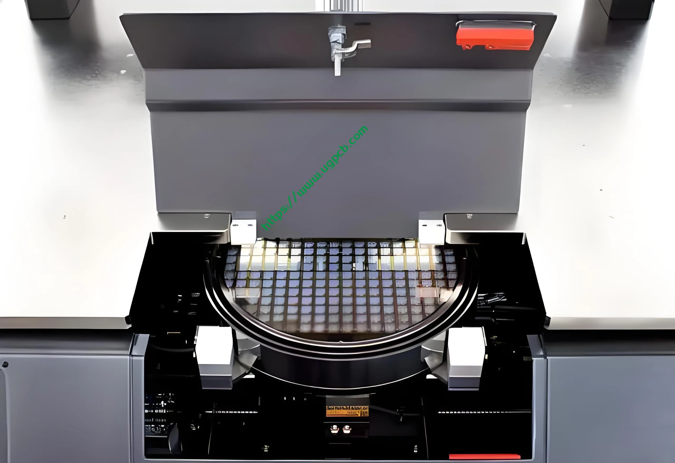
Сценарии приложения
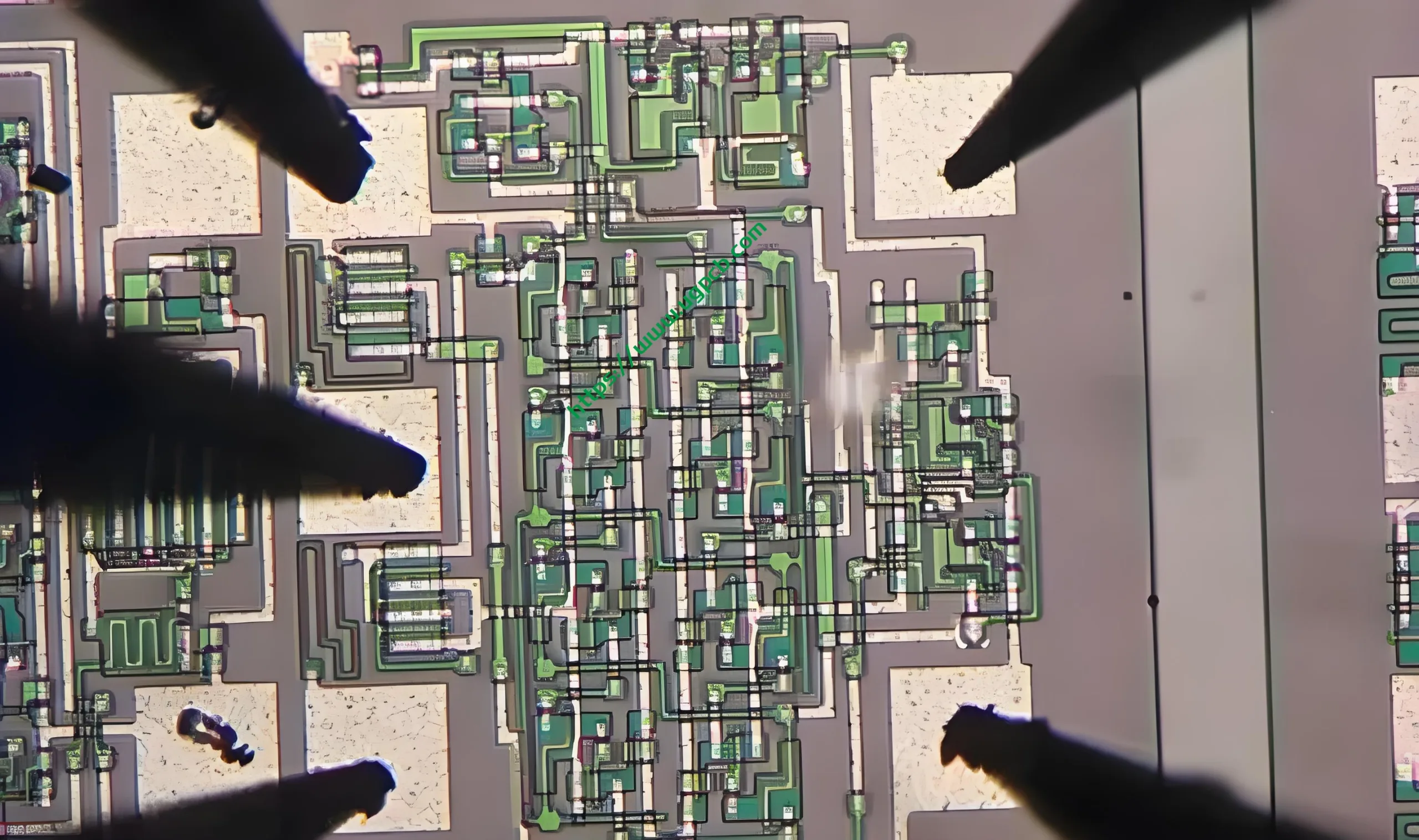
ATE test chip PCBs are primarily used in automated test equipment systems for the testing and validation of semiconductor chips. Они необходимы в полупроводниковой промышленности, where high-reliability testing is crucial for ensuring the quality and performance of chips before they are integrated into electronic devices. By utilizing ATE test chip PCBs, manufacturers can quickly and accurately identify any defects or issues in the chips, ensuring that only high-quality products are shipped to customers.


