
Overview of Burn-in Board
The Burn-in Board is a specialized type of PCB (Печатная плата) designed for IC burn-in test applications, also known as BIB (Burn-In Board) печатная плата. It undergoes rigorous testing to ensure the reliability and longevity of integrated circuits (ICS) before they are deployed in electronic devices.
Purpose of Burn-in Board
The primary purpose of a Burn-in Board is to subject ICs to accelerated aging conditions in order to identify potential early failures. This process helps in filtering out defective components before they are integrated into larger systems, thus reducing the overall failure rate and improving product quality.
Classification of Burn-in Board
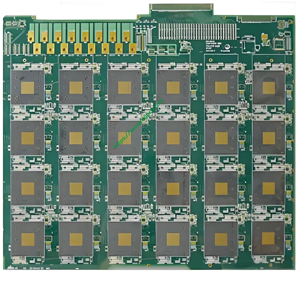
Burn-in Boards can be classified based on various factors such as the number of layers, material used, размер, и конкретные требования к применению. Our Burn-in Board, for instance, is a 20-layer PCB designed specifically for IC burn-in tests.
Материальная композиция
The Burn-in Board is manufactured using High TG TG175 material, which stands for high glass transition temperature. This material ensures that the board can withstand higher temperatures during the burn-in process without compromising its structural integrity.
Спецификации производительности
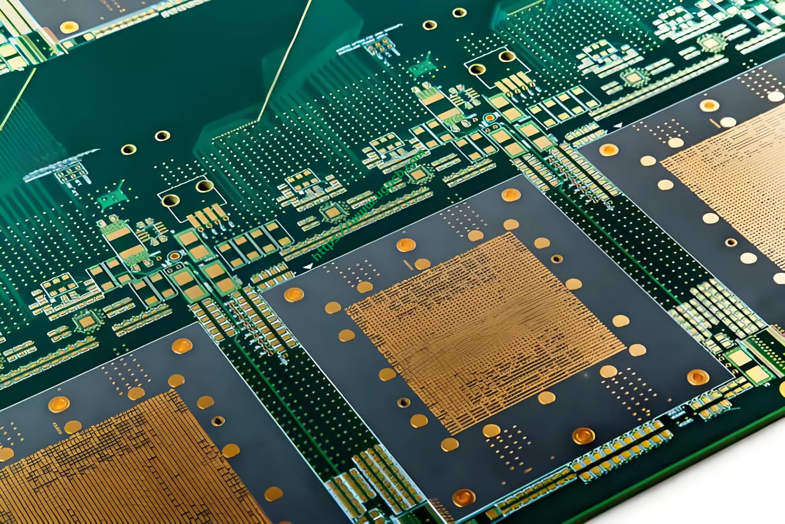
Our Burn-in Board boasts impressive performance specifications, including a board thickness of 3.2mm, a size of 610 * 572мм, and a BGA number of 24. It features immersion gold surface technology (3U) for enhanced conductivity and corrosion resistance. The copper thickness is optimized for both inner and outer layers, with 70/35um for inner layers and 35um for the outer layer.
Структурный дизайн
The structural design of the Burn-in Board is tailored to meet the rigorous demands of IC burn-in testing. The 20-layer construction provides ample routing space and electrical isolation, ensuring reliable performance during the test. The green color of the board aids in visual inspection and identification.
Ключевые особенности
Some of the notable features of our Burn-in Board include its high TG material, which allows for higher temperature operation, and the immersion gold surface finish, which ensures excellent electrical contact and corrosion resistance. Кроме того, the board’s design supports a high number of BGA components, making it suitable for complex IC testing applications.
Производственный процесс
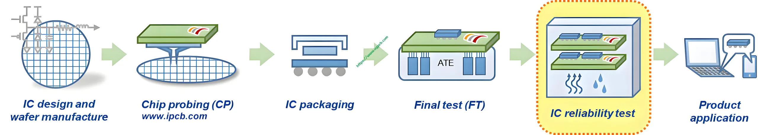
The production of a Burn-in Board involves several steps, including raw material preparation, ламинирование, бурение, copper plating, травление, and surface finish application. Each step is carefully monitored to ensure compliance with quality standards and customer specifications. After production, the boards undergo rigorous testing to verify their performance and reliability.
Сценарии приложения
Burn-in Boards are widely used in the electronics industry, particularly in the manufacturing and testing of ICs. They are essential for companies that produce high-reliability electronic devices, such as automotive, аэрокосмический, and medical equipment manufacturers. By using Burn-in Boards, these companies can ensure the quality and reliability of their products before they reach the market.


