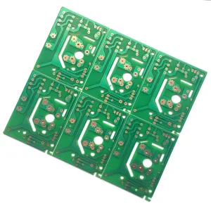
Introduction to FR4 PCB Circuit Board Material Composition
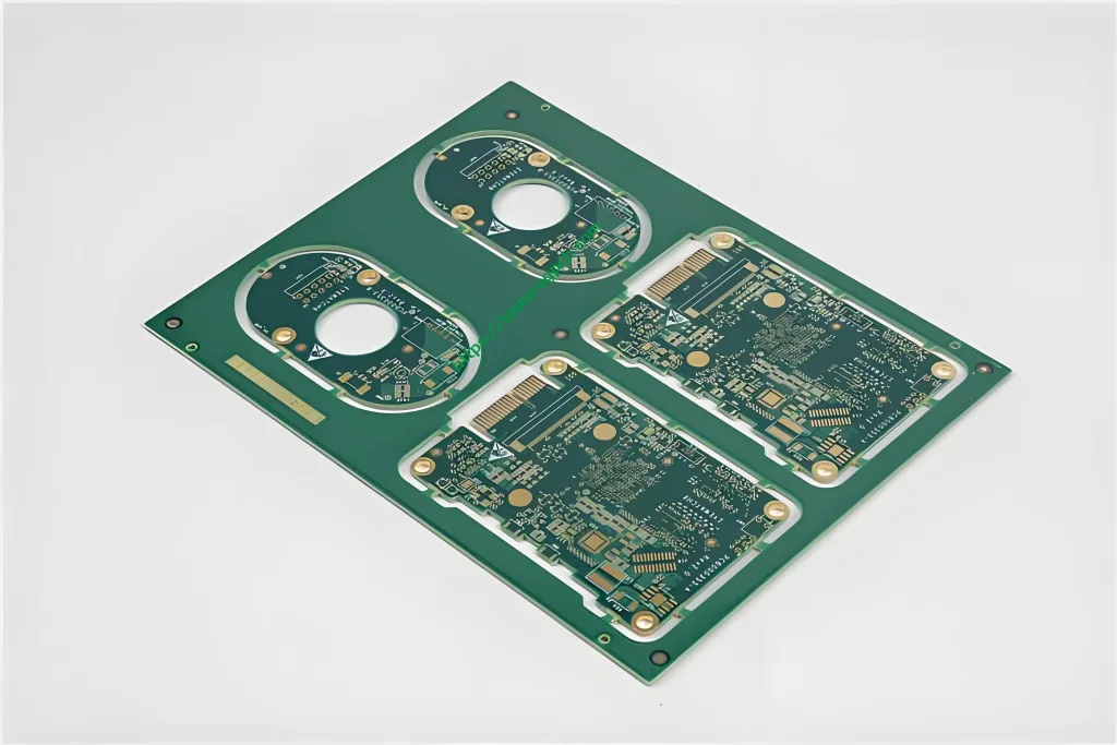
The FR4 PCB Circuit Board is primarily made of FR-4, a flame-retardant grade of epoxy resin-impregnated woven glass fiber cloth. This material offers exceptional electrical insulation and mechanical strength, making it ideal for a variety of electronic applications.
Характеристики производительности
FR4 PCB boards exhibit high temperature resistance, пламенная задержка, and excellent dimensional stability. They can withstand temperatures up to 130°C and maintain their structural integrity under thermal stress. The material’s low moisture absorption ensures reliable electrical performance in humid environments.
Структурный дизайн
The board is a 2-layer FR4 PCB, which means it has two conductive layers separated by a dielectric layer of FR-4 material. This design allows for the routing of circuits on both sides of the board while maintaining electrical isolation between them.
Color Options and Dimensions
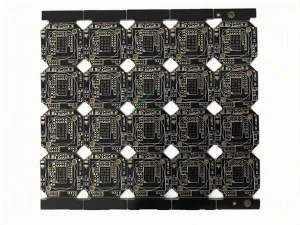
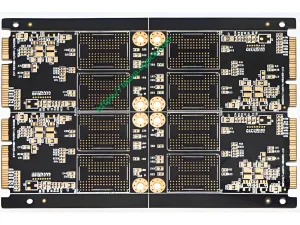
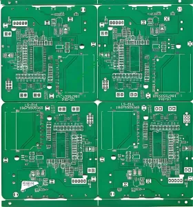
Available in various colors including green, черный, blue, and white, the FR4 PCB Circuit Board has a finished thickness of 1.20mm. The copper thickness is 1/1 ОЗ, providing a good balance between conductivity and cost.
Surface Finishes
The board’s surface can be treated with Immersion Gold or HASL (Hot Air Solder Leveling). Immersion Gold offers a high-quality finish suitable for sensitive applications requiring corrosion resistance and low contact resistance. ХАСЛ, on the other hand, is a cost-effective choice that provides a solderable surface with good electrical conductivity.
Производственный процесс
The production of FR4 PCB Circuit Boards involves several steps:
- Preparation of artwork and design layout.
- Etching of copper clad laminate to form the desired circuit patterns.
- Drilling of holes for component leads and vias.
- Plating of holes and surfaces to ensure electrical conductivity.
- Application of surface treatments like Immersion Gold or HASL.
- Final inspection and testing to ensure quality.
Сценарии приложения
The versatility of FR4 PCB Circuit Boards makes them suitable for a wide range of applications. They are commonly used in Wifi modules, where their reliable electrical performance and high temperature resistance are crucial. They are also ideal for electrical apparatus that requires robust and cost-effective circuit boards. In these applications, the FR4 PCB Circuit Board’s ability to withstand thermal stress and maintain dimensional stability ensures reliable operation over time.
 ЛОГОТИП УГКПБ

