
Low CTE and High Modulus
- Low CTE and high modulus, which can effectively reduce the warpage of the package carrier
- Excellent heat and humidity resistance
- Good PCB processability
-
Halogen-free materials
Application Field
eMMC and DRAM
- EMMC, DRAM
AP and PA
- AP, PA
Dual CM
- Dual CM
Fingerprint and RF Module
- Fingerprint, Радиочастотный модуль
Thermal and Mechanical Properties
- Тг (прямой доступ к памяти): 280 градус Цельсия
- Тд (5% мастерская. потеря): >400 градус Цельсия
- КТР (X/Y-axis) before Tg: 10 PPM/степень по Цельсию
- КТР (ось Z) α1/α2: 25/135 PPM/степень по Цельсию
- Диэлектрическая проницаемость (1ГГц): 4.4
- Коэффициент рассеяния (1ГГц): 0.007
- Прочность на очистку (1/3 ОЗ, VLP Cu): 0.80 N/мм
- Solder Dipping (@288 degree Celsius): >30 мин
- Young’s modulus (50 градус Цельсия): 26 Средний балл
- Young’s modulus (200 градус Цельсия): 23 Средний балл
- Flexural Modulus (50 градус Цельсия): 32 Средний балл
- Flexural Modulus (200 градус Цельсия): 27 Средний балл
Water Absorption and Flammability
- Водяной поглощение (А): 0.14%
- Водяной поглощение (85 degree Celsius/85%RH, 168Hr): 0.35%
- Воспламеняемость (UL-94): В-0
Other Properties
- Теплопроводность: 0.61 W/(m.K)
- Цвет: Черный
Введение
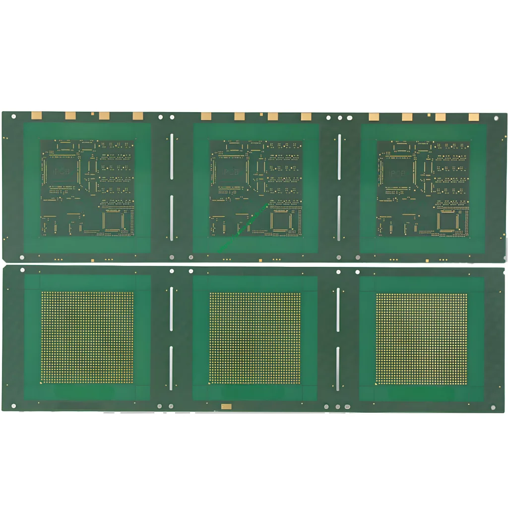
IC carrier board packaging frame refers to a key special basic material used for IC card module packaging. It mainly protects the chip and serves as the interface between the integrated circuit chip and the outside world. Его форма - лента, usually golden yellow.
Usage Process
The specific usage process is as follows: Первый, Чип карты IC прикреплен к раме упаковки карты IC полностью автоматической машиной размещения, И тогда контакты на чипе IC подключены к узлам на раме упаковки карты IC с помощью соединительной машины. Подключение цепи, и, наконец, использование упаковочных материалов для защиты интегрированной цепной чипы для формирования модуля интегрированной цепной карты, что удобно для последующих применений.
BGA Architecture и производственный процесс
Плата перевозчиков IC также является продуктом, основанным на BGA (Шариковая сетка массив) архитектура. Процесс производства аналогичен продуктам PCB, Но точность значительно улучшена. Процесс производства отличается от печатной платы. IC Substrate стал ключевым компонентом в упаковке IC, Постепенно заменить часть свинцовой рамки (Ведущий кадр) application.
Интегрированная схема
An integrated circuit integrates a general-purpose circuit on a chip. It is a whole. Once it is damaged internally, the chip is also damaged.
Печатная плата
The PCB can solder the components by itself, and replace the components if it is broken.
IC Carrier Board
В целом, the carrier board on the chip, the board is very small, usually the size of a 1/4 fingernail, the board is very thin (0.2~0.4mm), the material used is FR-5, BT resin, and the circuit is 2mil/About 2mil. It is a high-precision board that used to be generally produced in Taiwan, but now it is trending towards the mainland. The industry’s yield rate is 75%. The unit price of this kind of board is very high, generally bought according to PCS.


