
Overview of High Frequency PCB
A high-frequency PCB is a specialized type of circuit board designed to operate at high frequencies, typically in the range of gigahertz (ГГц). These PCBs are essential for applications that require precise signal transmission and minimal signal loss. They are widely used in industries such as telecommunications, радиолокационные системы, and satellite communications. The quality standard for high-frequency PCBs is IPC 6012 Сорт 2, ensuring high reliability and performance.
Определение и ключевые спецификации
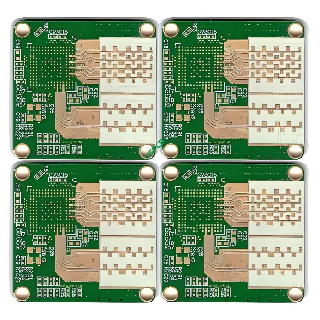
A high-frequency PCB is defined by its ability to handle signals at very high frequencies while maintaining signal integrity. Диэлектрическая проницаемость (дк) of these PCBs ranges from 2.0 к 1.6, which is crucial for controlling signal speed and impedance. The number of layers can vary from 1 к 36, providing flexibility for different design requirements. The thickness of the PCB ranges from 0.254mm to 12mm, and the copper thickness can be either 0.5oz or 1oz. Surface technologies include Silver, Золото, and OSP, each offering different benefits in terms of solderability and corrosion resistance. Special processes like mixed materials and stepped grooves further enhance the performance of high-frequency PCBs.
Соображения дизайна
When designing a high-frequency PCB, Несколько факторов должны быть рассмотрены:
- Диэлектрическая проницаемость (дк): The dk value between 2.0 и 1.6 is critical for maintaining signal integrity at high frequencies.
- Количество слоев: The wide range of layer options (1 к 36) allows for customization based on specific application needs.
- Толщина: The thickness range from 0.254mm to 12mm provides flexibility in design, catering to different spatial and functional requirements.
- Толщина меди: The choice between 0.5oz and 1oz base copper affects the current-carrying capacity and signal integrity.
- Surface Technology: Options like Silver, Золото, and OSP provide different levels of solderability and corrosion resistance.
- Специальные процессы: Techniques like mixed materials and stepped grooves can significantly enhance the performance of high-frequency PCBs.
Принцип работы
High-frequency PCBs operate based on the principle of controlled impedance and minimal signal loss. The dielectric constant of the materials used ensures that signals travel with minimal delay and loss, поддержание их целостности. Точный контроль над толщиной и массой меди допускает последовательный импеданс, что имеет решающее значение для высокочастотной передачи сигнала. Surface technologies like Silver, Золото, and OSP provide reliable connection points for components, Обеспечение эффективного передачи сигнала.
Приложения
High-frequency PCBs are used in a variety of applications that require high-speed data transmission and signal integrity:
- Телекоммуникации: Ensuring clear and reliable signal transmission in mobile phones, base stations, and other communication devices.
- Радиолокационные системы: Providing accurate and reliable signal processing in military and civilian radar systems.
- Спутниковая связь: Facilitating rapid and reliable data transfer between ground stations and satellites.
Классификация
High-frequency PCBs can be classified based on several criteria:
- Частотный диапазон: Typically operating at gigahertz (ГГц) frequencies.
- Количество слоев: От 1 к 36 слои, в зависимости от сложности схемы.
- Толщина: Options from 0.254mm to 12mm allow for customization based on specific application needs.
- Толщина меди: Standard and heavy copper options (0.5oz and 1oz) cater to different current-carrying capacities.
- Surface Technology: Choices like Silver, Золото, and OSP provide different levels of solderability and corrosion resistance.
Свойства материала
The key properties of high-frequency PCB materials include:
- Низкая диэлектрическая постоянная: Обеспечивает минимальную задержку и потери сигнала, making them suitable for high-frequency applications.
- Широкий диапазон толщины: Позволяет гибкости в дизайне, catering to different spatial and functional requirements.
- Excellent Signal Integrity: Поддерживает целостность сигнала даже на высоких частотах, обеспечение надежной производительности.
- Reliable Connection Points: Surface technologies like Silver, Золото, and OSP provide strong and reliable connection points for components.
Производственный процесс
The production of a high-frequency PCB involves several steps:
- Выбор материала: Choosing materials with a low dielectric constant and high signal fidelity.
- Конструкция схемы: Создание схемы схемы с соображениями для высокочастотной производительности и целостности сигнала.
- Офорт: Удаление ненужной меди для создания желаемой схемы схемы.
- Ламинирование: Соединение нескольких слоев вместе под высоким давлением и температурой, чтобы обеспечить прочное и надежное соединение.
- Поверхностная отделка: Applying surface technologies like Silver, Золото, or OSP to enhance solderability and corrosion resistance.
- Специальные процессы: Utilizing techniques like mixed materials and stepped grooves to further enhance performance.
- Тестирование и контроль качества: Обеспечение конечного продукта соответствует всем спецификациям и стандартам.
Используйте сценарии
High-frequency PCBs are used in scenarios where high-speed data transmission and signal integrity are critical:
- Mobile Phones: Ensuring clear and reliable signal transmission in modern smartphones.
- Base Stations: Providing accurate and reliable signal processing in communication infrastructure.
- Радиолокационные системы: Enabling precise and reliable signal processing in military and civilian radar applications.
- Спутниковая связь: Facilitating rapid and reliable data transfer between ground stations and satellites.
В итоге, high-frequency PCBs are specialized circuit boards designed for high-speed data transmission and signal integrity. Their low dielectric constant, широкий диапазон толщины, and excellent signal fidelity make them ideal for applications in telecommunications, радиолокационные системы, and satellite communications.


