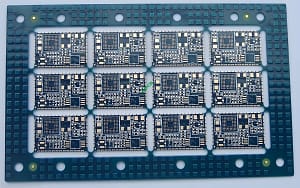
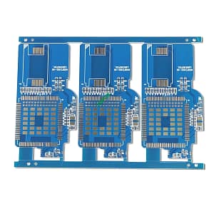
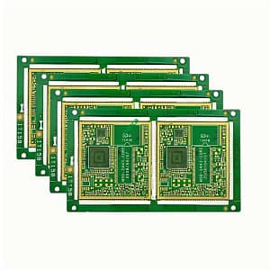
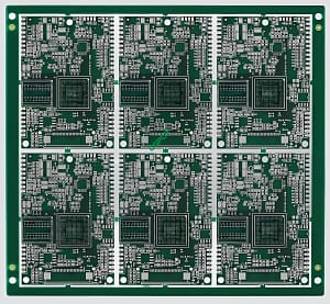
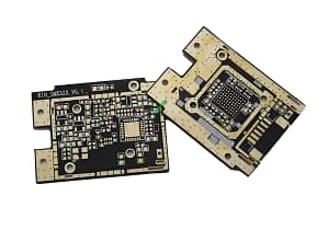
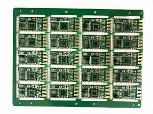
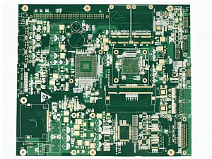
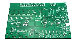
1. For PCB boards that require frequent insertion and removal, it is generally necessary to harden the gold fingers through a plating process to enhance their wear resistance.
2. The gold fingers need to be angled backwards, typically at 45°. Other angles such as 20°, 30°, и т. д., are also used. If the design does not include this backward angle, there is an issue. As shown in the diagram below, the arrow indicates a 45° back tilt:
3. A complete solder mask window should be created for the gold fingers. No need to open the steel mesh for the pins;
4. The minimum distance between Shenxi and Shenyin pads is 14 миллион. It is recommended that the solder pads are more than 1mm away from the finger position, including through-hole solder pads;
5. Do not apply copper coating on the surface of the gold fingers.
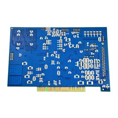
Многослойная плата управления материнской платой с золотыми пальцами
- Подробная информация о продукте
Предыдущий: Многослойная печатная плата для средств связи
Следующий: Двусторонняя печатная плата FR4 с золотым пальцем
 ЛОГОТИП УГКПБ

