
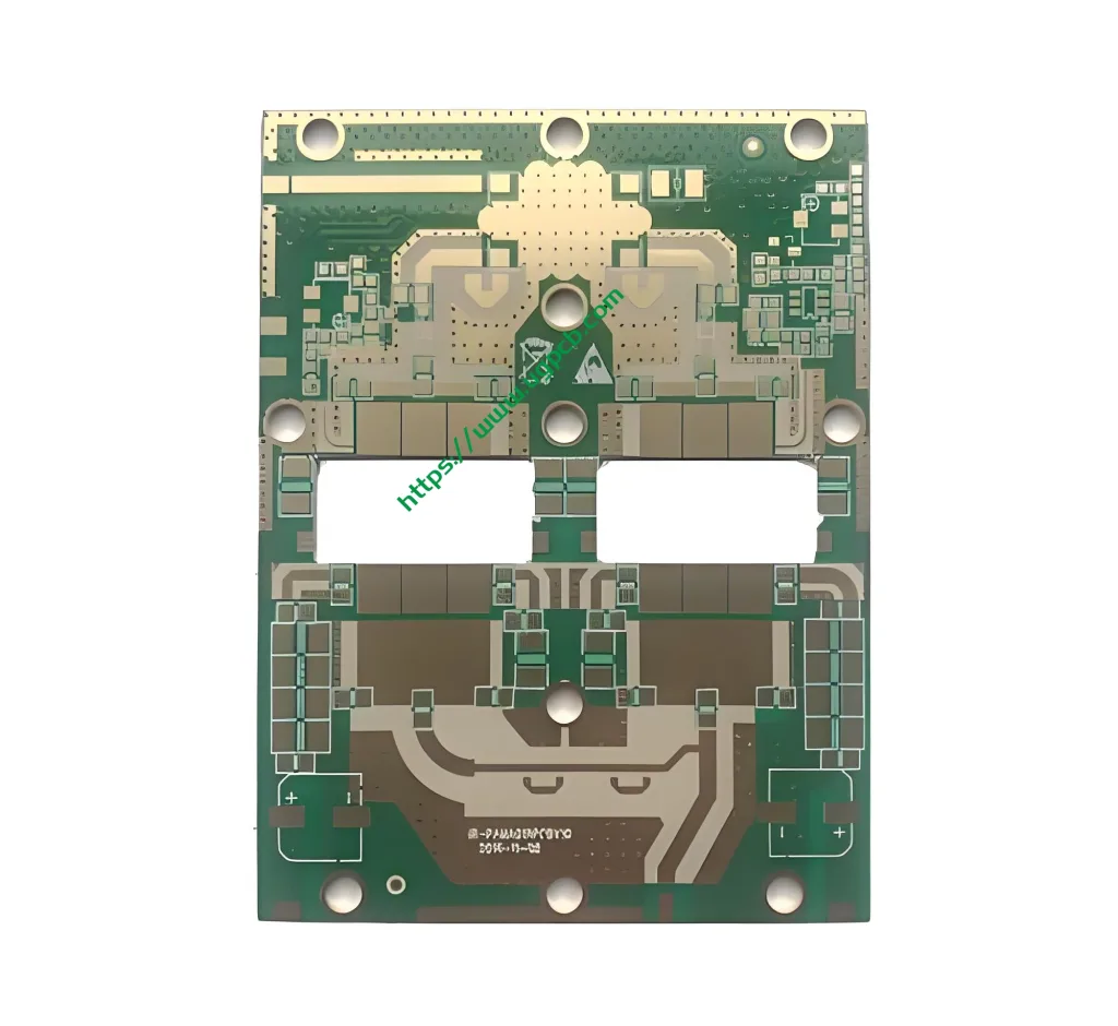
Overview of RF Circuit PCB
Радиочастота (РФ) Circuit Printed Circuit Boards, or RF PCBs, are specialized boards designed for high-frequency applications. They play a critical role in ensuring signal integrity and minimizing loss in devices operating at microwave frequencies. These boards are integral to the performance of antennas, инструменты, and various communication equipment.
Definition and Design Considerations
An RF PCB is a type of circuit board specifically engineered to handle high-frequency signals, typically in the range of megahertz (МГц) to gigahertz (ГГц). Key design considerations include:
- Dielectric Material: The choice of material affects signal propagation speed and loss.
- Толщина меди: Determines current-carrying capacity and thermal management.
- Layer Stack-Up: Influences impedance control and crosstalk.
Working Principle and Applications
RF PCBs operate based on the principles of electromagnetic wave propagation. At high frequencies, even minor imperfections can significantly impact signal quality. Поэтому, these boards are designed with precision to maintain controlled impedance and minimize insertion loss. Applications include:
- Antennas: Ensuring efficient transmission and reception of signals.
- Инструменты: Providing accurate measurements in test and measurement equipment.
- Communication Equipment: Facilitating reliable data transfer in wireless systems.
Classification and Materials
Типы:
- Single-Sided and Double-Sided RF PCBs: Suitable for simpler designs with fewer layers.
- Multilayer RF PCBs: Offer more complexity and better performance for advanced applications.
Core Materials:
- ФР-4: A common material known for its cost-effectiveness and reliability.
- Teflon/PTFE: Offers low dielectric constant and loss tangent, ideal for high-frequency applications.
- Ceramic/Hydrocarbon: Provides excellent thermal stability and mechanical strength.
Performance and Structure
Key performance indicators for RF PCBs include:
- Диэлектрическая проницаемость (Дк): Ranges from 2.0 к 1.6, affecting signal speed and impedance.
- Толщина: Varies from 0.254mm to 12mm, influencing the board’s mechanical stability and layer count.
- Толщина меди: Typically ranges from 0.5oz to 2oz, impacting current handling and heat dissipation.
The structure of an RF PCB includes multiple layers of conductive pathways embedded within the dielectric material, often with precise impedance control and strict tolerances to ensure optimal signal integrity.
Characteristics and Production Process
RF PCBs are characterized by:
- Strict Tolerance Control: Ensuring consistent electrical performance across all units.
- High-Quality Standards: Adhering to IPC Class 2 or Class 3 стандарты.
The production process involves several stages:
- Выбор материала: Choosing the right substrate and copper foil based on application requirements.
- Паттерн схемы: Using photolithography to create precise circuit patterns.
- Офорт: Removing unwanted copper to form the desired circuitry.
- Покрытие: Applying surface finishes like silver, gold, or OSP for corrosion resistance and better solderability.
- Гарантия качества: Conducting rigorous testing to ensure compliance with specifications.
Используйте сценарии
RF PCBs are essential in scenarios where signal quality and integrity are paramount. Some examples include:
- Wireless Communications: Enabling clear and reliable transmission in mobile phones, Wi-Fi routers, and other wireless devices.
- Радиолокационные системы: Providing precise signal handling for detection and ranging.
- Medical Devices: Ensuring accurate data collection and analysis in diagnostic equipment.
В итоге, RF Circuit PCBs are specialized boards designed for high-frequency applications, requiring meticulous attention to detail in their design and manufacturing. They offer superior performance in terms of signal integrity and are crucial in various industries, including telecommunications, аэрокосмический, and medical technology.


