Введение
The standard ClearONE terminator is the industry leader in performance and reliability. The need to provide a lead-free solution for resistor terminator networks in compliance with the RoHS initiative has required CTS to add a new material set to the ClearONE product line.
Lead Elimination in BGA Products
Many manufacturers have chosen to utilize Tin/Silver/Copper (Sn/Ag/Cu or SAC) spheres in their BGA products as a means of eliminating lead. The SAC spheres collapse into the interface solder during the reflow process, providing an unwanted and less than desirable variation in performance.
RoHS ClearONE Material Set
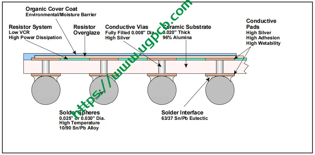
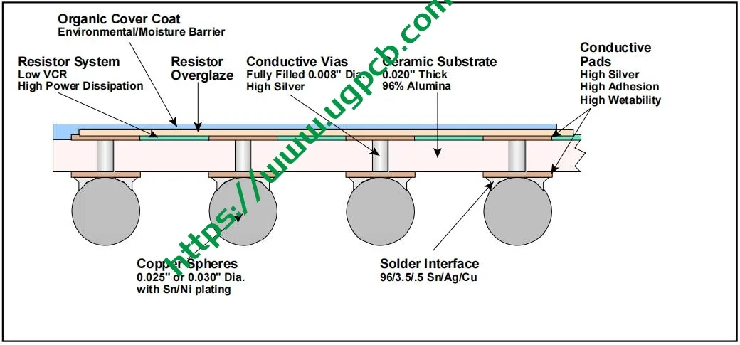
This new RoHS ClearONE material set takes advantage of the existing designs while eliminating lead-bearing solders. ClearONE solder spheres (10/90 Tin/Lead) and the eutectic interface solder (63/37 Tin/Lead) are replaced with Tin/Nickel-plated copper spheres and high-temperature Tin/Silver/Copper (Sn/3.5Ag/0.5Cu) interface solder for the RoHS ClearONE terminators. As with the 10/90 spheres, the copper spheres do not collapse during solder reflow. By utilizing spheres that do not collapse, the RoHS ClearONE terminators maintain a predictable, consistent standoff height, and the performance established in the previous non-RoHS product.
Standard ClearONE BGA Terminator Material Set
The standard ClearONE Ball Grid Array (БГА) terminator material set is described in Figure 1. The ClearONE product designs provide identical performance in each channel through the use of symmetrical element layouts and by maintaining predictable standoff spacing.
RoHS Compliant ClearONE Terminators
The RoHS Compliant ClearONE terminators continue to take advantage of the symmetrical layout designs and predictable standoff spacing by utilizing copper spheres that maintain their shape, как показано на рисунке 2.
Description
PCB Land Pad Design
Shape and Diameter
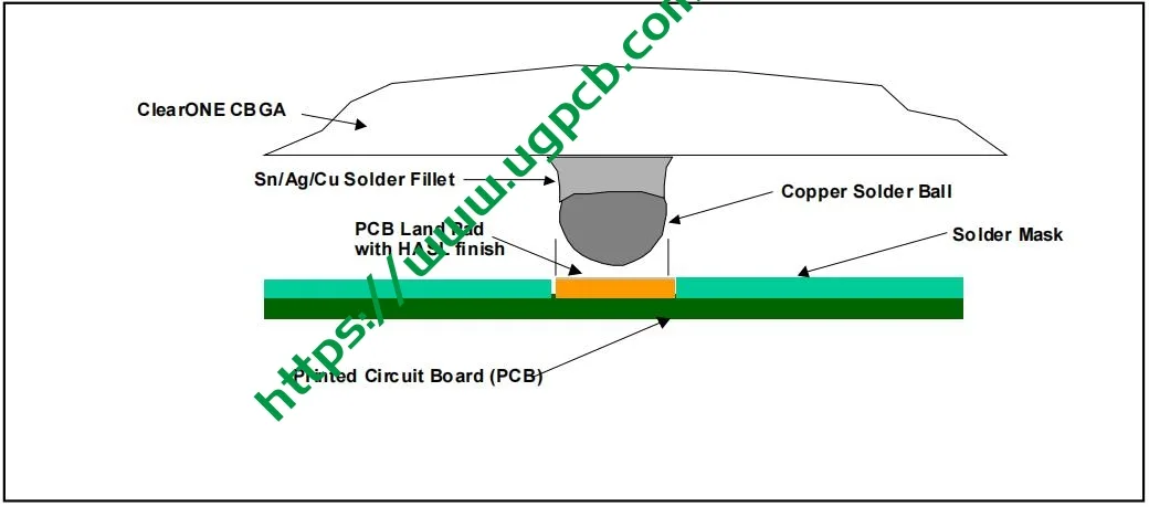
The shape of the CBGA land pads on the PCB should be round. The diameters of the PCB land pads are recommended to be equal to the nominal CBGA solder ball diameter as provided on the product data sheets, see Figure 3. Tolerance for the CBGA land pad diameter is + 0.001 дюймы (+0.025мм). The absolute minimum land pad diameter shall be 0.020” and 0.025” for 1.0mm and 1.27mm pitch parts respectively.
Припаяя маска
The solder mask surrounding the land pad should not overlap the land pad to ensure maximum thermal cycling reliability, see Figure 3.
Electrical Trace
The electrical trace leading into the CBGA land pads requires a minimum width trace per the PCB board manufacturing technology used.
Vias
CBGA land pads are not to be located on top of any vias. Vias connected to the CBGA land pads should have a minimum width connecting trace, with a minimum length of 0.010 дюймы (0.254 мм), see Figure.
RoHS Custom Quick Turn PCB Manufacturing and Assembly
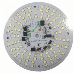
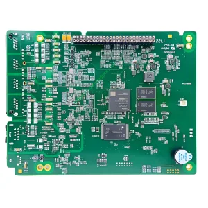
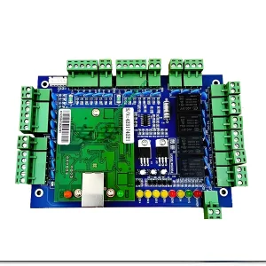
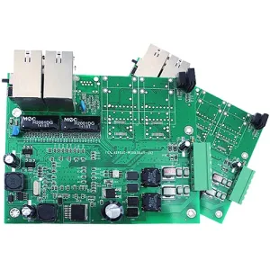
UGPCB supports RoHS Custom Quick Turn PCB Manufacturing and PCB Assembly business. We are a professional PCBA one-stop assembly factory. Welcome to place an order.
 ЛОГОТИП УГКПБ
