
Знакомство с печатной платой камеры наблюдения UGPCB
Печатная плата камеры наблюдения UGPCB представляет собой высокопроизводительную печатная плата разработан специально для приложений безопасности и мониторинга. Этот печатная плата использует передовые материалы и производственные процессы для обеспечения надежности в сложных условиях. В качестве ключевого компонента современных систем наблюдения., он поддерживает растущий спрос на межсоединения высокой плотности (ИЧР) дизайн, что делает его идеальным для компактного и эффективного печатная плата собрания. С такими функциями, как обработка поверхности иммерсионным золотом, а также слепые и потайные переходные отверстия., эта плата является примером инноваций в технологии печатных плат для индустрии безопасности..

Что такое печатная плата камеры наблюдения?
Печатная плата камеры наблюдения — это специализированная печатная плата, которая составляет основу систем камер видеонаблюдения., облегчение подключения и эксплуатации электронных компонентов, таких как датчики, процессоры, и модули связи. Он определяется его способностью обрабатывать высокоскоростные сигналы и распределять мощность, сохраняя при этом стабильность в различных условиях.. Этот тип печатной платы необходим для преобразования необработанных данных в полезную информацию в приложениях наблюдения., а версия UGPCB выделяется благодаря своей индивидуальной конструкции для создания изображений с высоким разрешением и обработки данных в реальном времени..
Ключевые аспекты проектирования печатных плат высокой плотности
Проектирование печатной платы камеры наблюдения требует внимания к нескольким критическим факторам для достижения оптимальной производительности.. Первый, след и пространство 3mil/3mil (0.075мм/0,075 мм) Требуйте точности в компоновке, чтобы предотвратить помехи и обеспечить целостность сигнала.. Второй, использование глухих и скрытых переходных отверстий обеспечивает эффективную разводку на многослойных платах., уменьшение размера платы и повышение надежности. Кроме того, готовая толщина 1,2 мм и вес меди в 1 унцию должны быть сбалансированы для обеспечения рассеивания тепла и механической прочности.. Разработчикам также следует учитывать контроль импеданса и экранирование от электромагнитных помех для поддержки высокочастотных операций, типичных для систем наблюдения PCBA., обеспечение совместимости с такими компонентами, как датчики изображения и беспроводные модули.
Как функционирует печатная плата в системах наблюдения
Принцип работы этой печатной платы основан на ее роли центральной нервной системы камеры наблюдения.. Он соединяет различные компоненты, например, датчик изображения, процессор, память, и коммуникационные интерфейсы, захватить, процесс, и передавать видеоданные. Электрические сигналы проходят через мелко расположенные дорожки и переходные отверстия., с поверхностью иммерсионного золота, обеспечивающей надежность паяных соединений и устойчивость к коррозии. Многослойная структура, включая слепые и скрытые переходные отверстия, обеспечивает эффективное распределение мощности и изоляцию сигналов, снижение шума и улучшение качества изображения. По сути, этот печатная плата для камер наблюдения действует как магистраль, поддержка мониторинга в реальном времени и хранения данных в сборках PCBA.
Приложения и использование в решениях безопасности
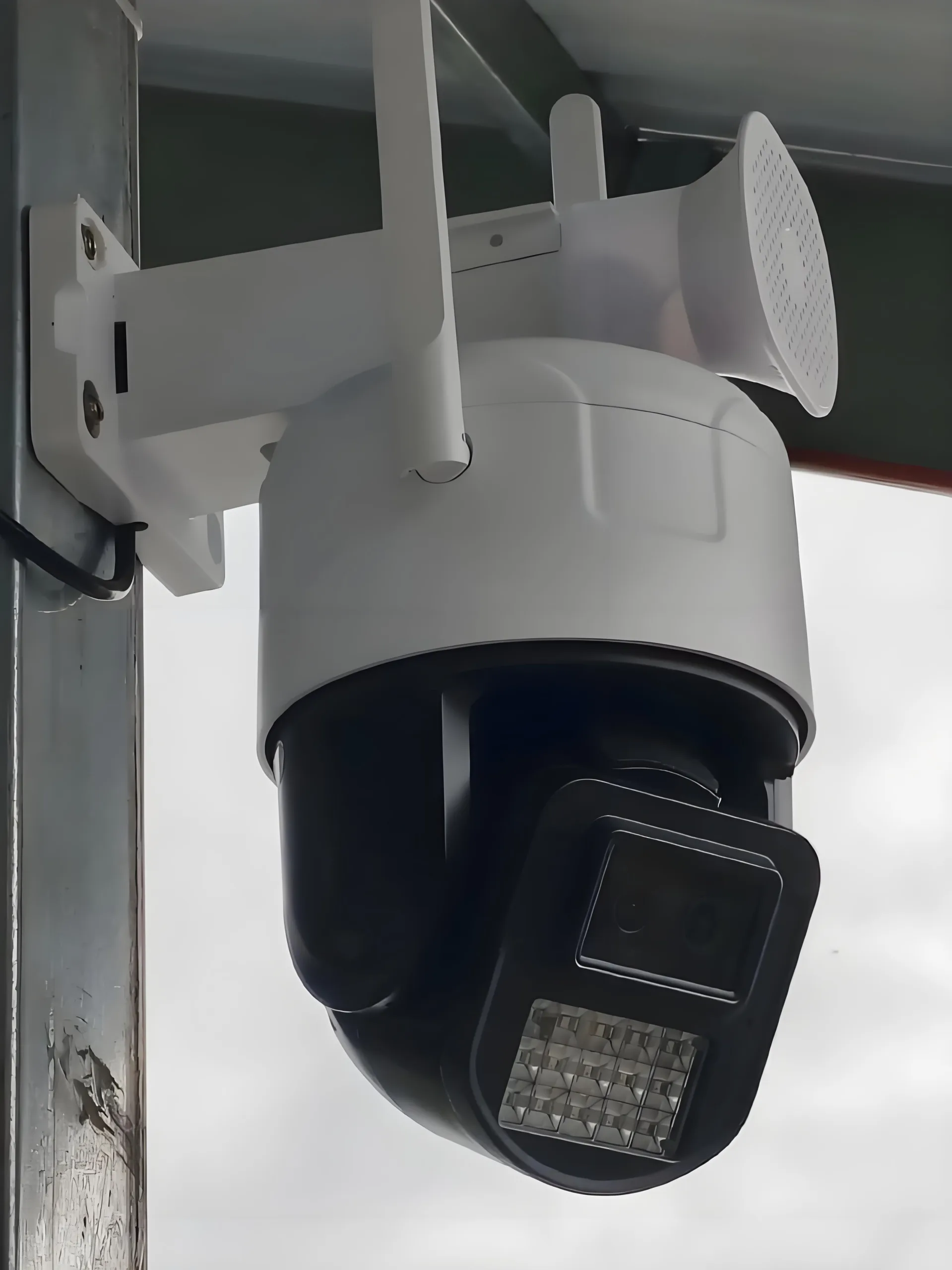
Эта печатная плата в основном используется в камерах наблюдения для широкого спектра приложений безопасности., включая системы домашней безопасности, коммерческий мониторинг, и инфраструктура общественной безопасности. Он включает такие функции, как ночное видение., обнаружение движения, и беспроводное соединение, что делает его универсальным для различных сред. За пределами камер, его можно интегрировать в соответствующие проекты PCBA, такие как видеорегистраторы и системы сигнализации.. Конструкция высокой плотности делает его подходящим для компактных устройств., поддержка тенденции к миниатюризации в электронной промышленности при сохранении высокой производительности для критически важных задач наблюдения.
Классификации типов печатных плат для наблюдения
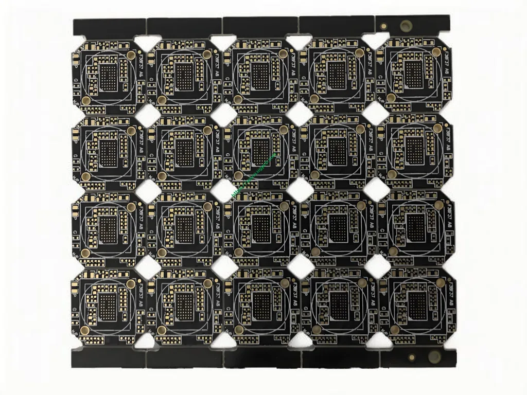
Печатные платы камер наблюдения можно классифицировать по нескольким критериям.. По количеству слоев, эта 6-слойная плата относится к категории многослойных, идеально подходит для сложных схем. На основе материала, он использует СИ С1000-2 ТГ170 ФР4, что классифицирует ее как печатную плату FR4 с высоким Tg, подходящую для приложений с высокими термическими требованиями.. Кроме того, наличие слепых и скрытых переходных отверстий ставит его в HDI печатная плата классификация, предназначен для передовых межсетевых решений. Эти категории помогают пользователям выбрать подходящую печатную плату для своих потребностей в печатных платах., обеспечение совместимости с конкретными моделями камер наблюдения и требованиями к производительности.
Материалы, используемые при изготовлении печатной платы
Печатная плата камеры наблюдения UGPCB изготовлена из материала SY S1000-2 TG170 FR4., высокоэффективный ламинат, известный своей термостабильностью (с температурой стеклования 170°С.) и отличная электроизоляция. Такой выбор материала гарантирует, что плата выдержит высокие температуры во время сборки и эксплуатации печатной платы., снижение риска расслоения или отказа. В сочетании с толщиной меди 1 унция, обеспечивает хорошую проводимость и долговечность, а обработка поверхности иммерсионным золотом улучшает паяемость и устойчивость к факторам окружающей среды., что делает его надежным выбором для долгосрочного использования в системах наблюдения..
Эксплуатационные характеристики и характеристики
Эта печатная плата обеспечивает исключительные показатели производительности., в том числе высокая термостойкость благодаря материалу TG170, что предотвращает деформацию под воздействием тепла. Траектория толщиной 3 мил и пространство обеспечивают высокоскоростную передачу сигнала с минимальными потерями., поддержка задач наблюдения с интенсивным использованием полосы пропускания. Электрические характеристики улучшаются за счет 6-слойной структуры., что обеспечивает лучшую помехоустойчивость и целостность питания. Минимальный размер отверстия 0,2 мм., обеспечивает плотное размещение компонентов, а покрытие иммерсионным золотом обеспечивает низкое контактное сопротивление.. Общий, эти характеристики делают ее лучшей печатной платой для камер наблюдения., обеспечение долговечности и эффективности интеграции PCBA.
Подробности конфигурации структуры и слоев
Плата имеет 6-слойную структуру со специальной конфигурацией слоев, включающей глухие переходы между слоями. 1-2 и 5-6, и скрытые переходные отверстия во внутренних слоях, как указано в 1-2,5-6,7-12 обозначение (где 7-12 может относиться к стандартизированной группировке внутренних слоев в проектах ИЧР.). Эта конфигурация оптимизирует пространство и улучшает маршрутизацию сигналов за счет уменьшения количества шлейфов.. Общая толщина 1,2 мм обеспечивает прочную основу., а медные слои обеспечивают равномерное распределение тока. Такой структурированный подход повышает надежность печатных плат в системах наблюдения., поддержка сложных макетов печатных плат без ущерба для производительности.
Основные характеристики печатной платы камеры наблюдения
Примечательные особенности этой печатной платы включают в себя возможность соединения высокой плотности с дорожкой и пространством 3 мил., что позволяет миниатюризировать и улучшить функциональность. Слепые и скрытые переходные отверстия позволяют создавать более компактные конструкции, освобождая место на поверхности для компонентов.. Обработка поверхности иммерсионным золотом обеспечивает превосходную коррозионную стойкость и паяемость., продление срока службы платы. Кроме того, использование материала SY S1000-2 TG170 FR4 обеспечивает высокие тепловые характеристики., что делает его пригодным для камер наружного наблюдения, подвергающихся воздействию различных температур.. В совокупности эти функции делают эту печатную плату идеальным выбором для передовых проектов PCBA в секторе безопасности..
Производственный процесс от проектирования до завершения
Производственный процесс начинается с проектирования и верстки., использование программного обеспечения САПР для реализации спецификаций трассировки и пространства толщиной 3 мил, а также путем размещения. Следующий, материал SY S1000-2 TG170 FR4 ламинирован и многослойен, со слепыми и скрытыми переходными отверстиями, просверленными лазерным или механическим методом. Затем медь покрывается слоем толщиной 1 унцию., с последующим нанесением рисунка и травлением для создания следов схемы.. Обработка поверхности иммерсионным золотом применяется для повышения проводимости и защиты.. Окончательно, плата проходит тестирование, включая электрические и визуальные проверки, чтобы убедиться, что он соответствует стандартам качества, прежде чем интегрировать его в сборки PCBA для камер наблюдения..
Сценарии использования в современном видеонаблюдении
Эта печатная плата используется в различных сценариях., например, камеры видеонаблюдения в жилых домах для мониторинга в режиме реального времени., Коммерческие здания для предотвращения краж, и общественные места для наблюдения за дорожным движением. Конструкция с высокой плотностью делает его идеальным для компактных, незаметные камеры, а прочная конструкция позволяет использовать его на открытом воздухе в суровых погодных условиях.. В проектах умного города, он упрощает объединение сетей наблюдения за счет надежной интеграции PCBA. Общий, а УГКПБ Печатная плата камеры наблюдения адаптируется к различным средам, обеспечение основы для инновационных решений безопасности, в которых приоритет отдается производительности и долговечности..


I will right away grab your rss feed as I can’t find your e-mail subscription link or e-newsletter service. Do you have any? Kindly let me know in order that I could subscribe. Thanks.