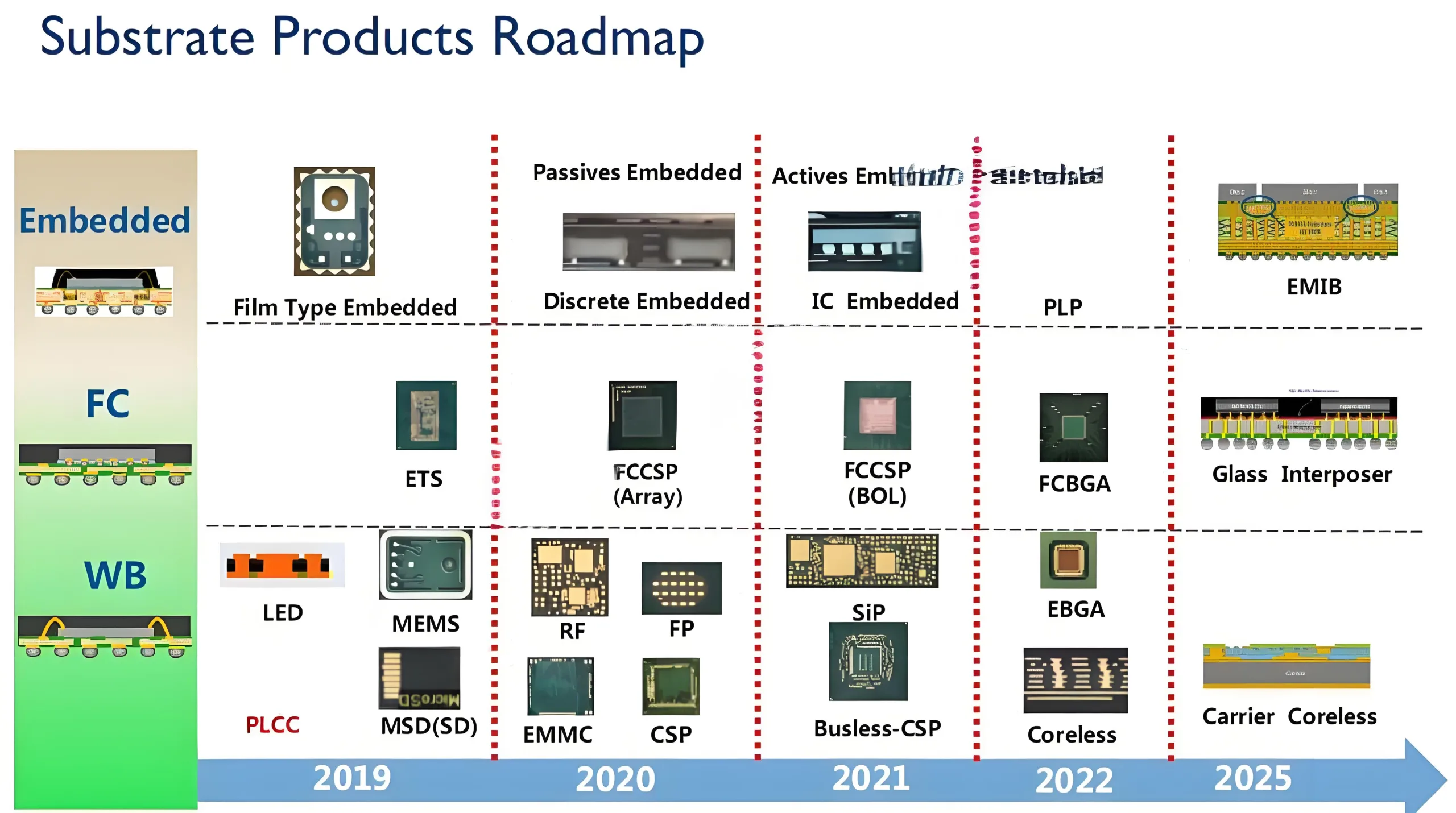
Substrate Products Roadmap

Substrate Products Roadmap
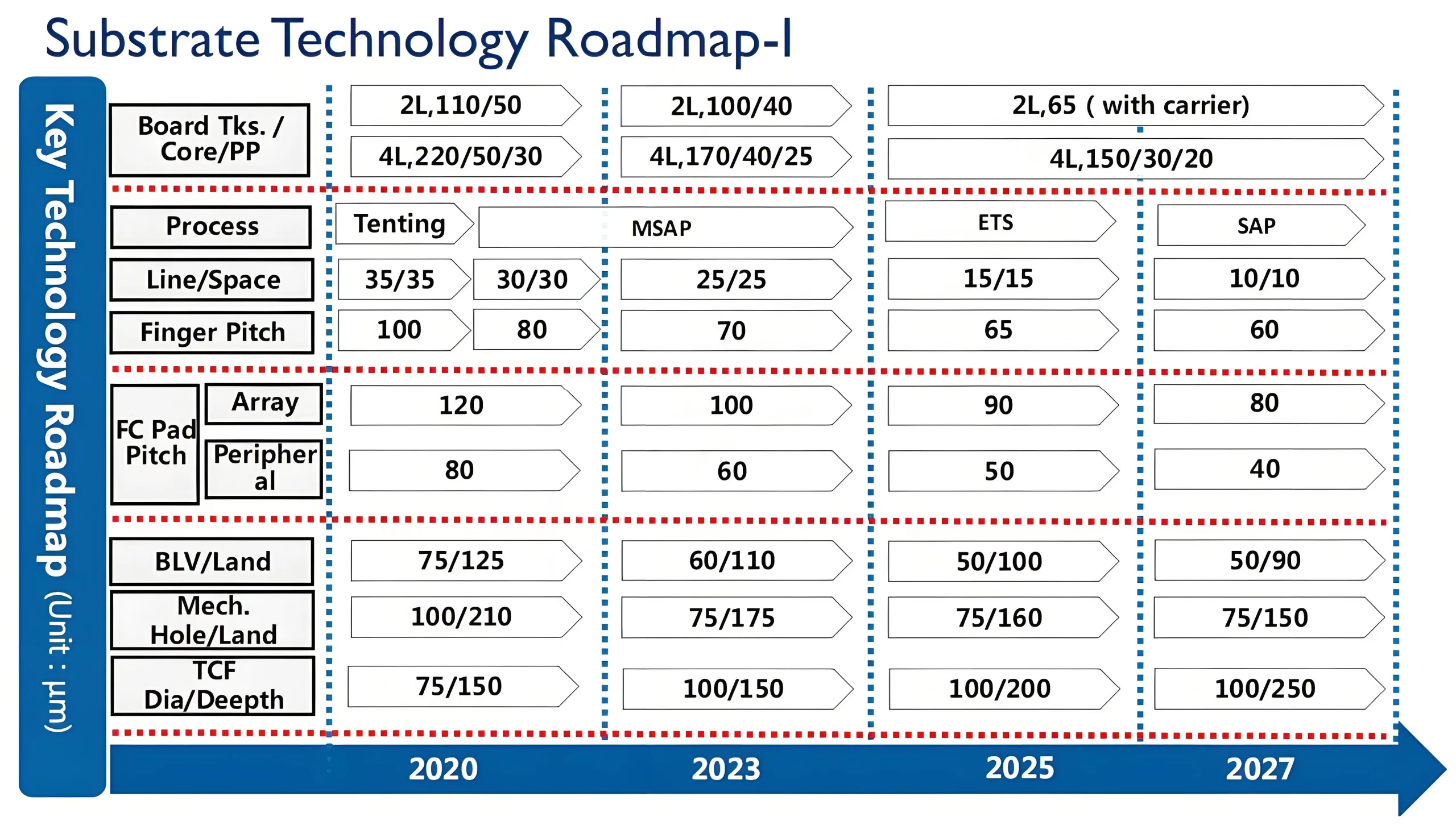
Substrate Technology Roadmap 1

Substrate Technology Roadmap 1
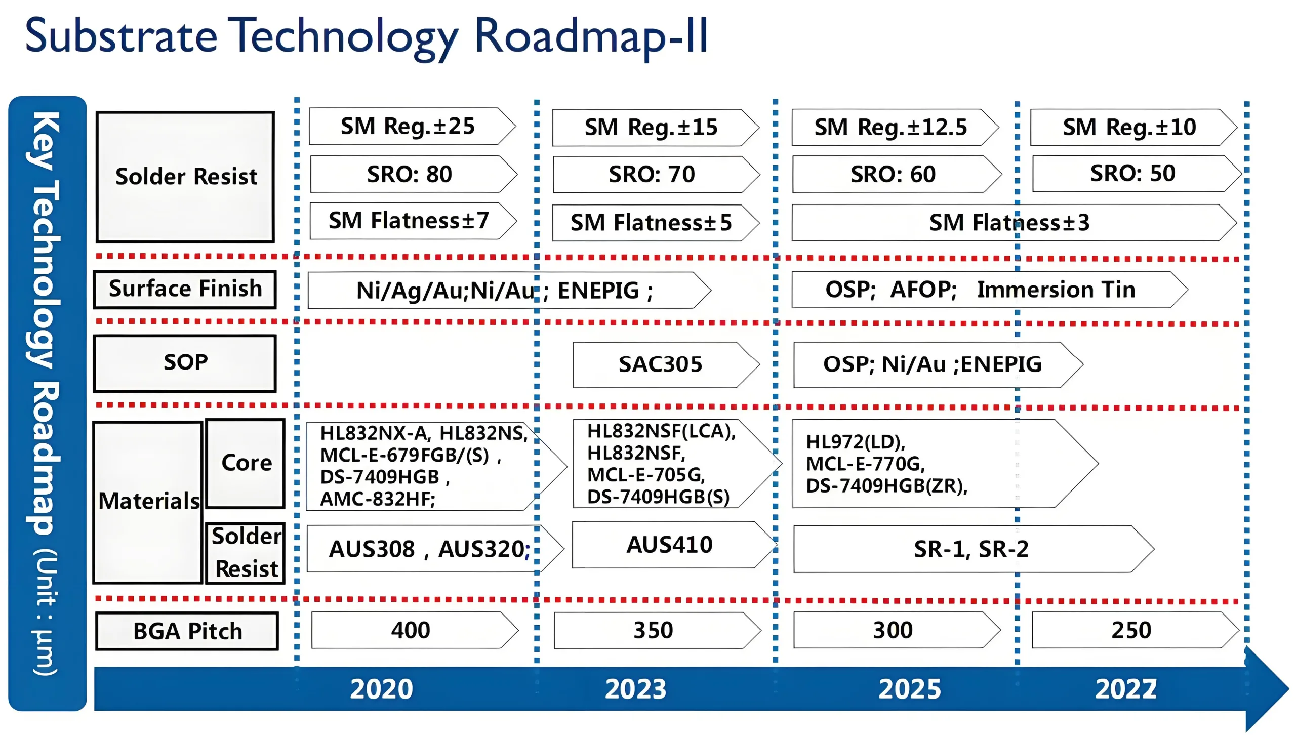
Substrate Technology Roadmap 2

Substrate Products Roadmap 2
System-in-Package Substrate (จิบ)
System-in-package is a system platform that assembles multiple heterogeneous wafers, sensing components, passive components, ฯลฯ, into one package. Its applications include multi-chip module (MCM), multi-chip package (MCP), stacked chip package, package in package (PiP), and embedded component carrier board. System-in-package provides IC system designers with another computing function integration solution besides System-on-Chip (SoC). It has the advantages of integrating heterogeneous chips from different sources, being smaller and thinner, and entering the market quickly.
SiP can be a multi-chip module (Multi-chip Module; MCM) planar 2D package, and can also reuse the 3D package structure to effectively reduce the packaging area and its internal bonding technology can be pure wire bonding (Wire Bonding), FlipChip can also be used, but the two can also be mixed. In addition to 2D and 3D packaging structures, another way of integrating components with multi-functional substrates can also be included in the scope of SiP. This technology mainly embeds different components in a multifunctional substrate, and can also be regarded as the concept of SIP to achieve the purpose of functional integration. Different chip arrangements and different internal bonding technologies enable SIP package types to produce diversified combinations. UGPCB can be customized or flexibly produced according to the needs of customers or products.
Plastic Ball Gate Array Package Substrate (PBGA)
This is the most basic ball gate array substrate used in wire bonding and packaging. Its basic material is a copper foil substrate impregnated with glass fiber. The plastic ball gate array packaging substrate can be applied to chip packaging with a relatively high pin count. When the chip function is upgraded, the traditional lead frame package structure becomes inadequate with the increase in the number of output/input pins, and the plastic ball gate array package substrate provides a cost-effective solution.
Flip Chip Chip Scale Package Substrate (FCCSP)
The semiconductor chip is not connected to the substrate by wire bonding but is interconnected with the substrate by bumps in a flip-chip state, so it is called FCCSP (Flip Chip Chip Scale Package). Flip-chip wafer-level size packaging will further show the cost advantage. In the recent past, the process cost of bumps on wafers has also continued to drop, which has also led to a faster reduction in packaging costs. Flip-chip chip-level size packaging has become a high-pin-count IC.
Flip Chip Ball Gate Array Package Substrate (FCBGA)
FC-BGA (Flip Chip-Ball Grid Array) substrate is a high-density semiconductor package substrate that can realize the high-speed and multi-functionalization of LSI chips. The flip-chip ball gate array package has very excellent performance and cost advantages in the package of very high output/input pin counts, such as a chip such as microprocessor or an image processor.
If you need IC substrate, please don’t hesitate to contact UGPCB, อีเมล: sales@UGPCB.com
 โลโก้ UGPCB

วีแชท
สแกนรหัส QR ด้วย WeChat