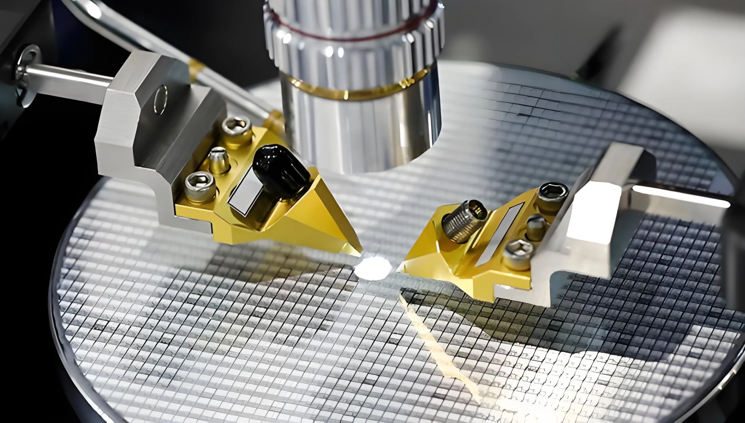
TSV and TGV 3D packaging
Packaging technology, as one of the core processes in the semiconductor industry, has witnessed the trend of miniaturization, high-density, and multifunctionality in electronic products. From through-hole packaging to surface-mount packaging, and then to BGA, CSP, SCM, MCM, WLP, 3D packaging, and SIP, every advancement in packaging technology has driven significant leaps in electronic products. Among these packaging technologies, Through Silicon Via (TSV) and Through Glass Via (TGV) technologies are undoubtedly the two key keys to unlocking the new era of 3D packaging.
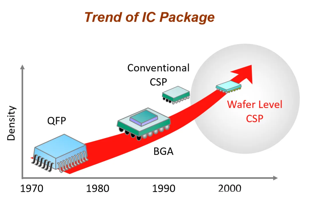
The development process of 3D packaging technology
3D Packaging: Forms and Interconnection Methods
3D packaging is mainly classified into three types: buried type, active substrate type, and stacked type. The buried type buries devices within multilayer wiring or within the substrate. The active substrate type first integrates components with a wafer substrate to form an active substrate, and then arranges multilayer interconnects. The stacked type involves stacking silicon wafers or chips. 3D interconnection methods include wire bonding, flip-chip, TSV, and thin-film conductors. ในหมู่พวกเขา, TSV enables vertical interconnection between chips, serving as a critical technology for achieving miniaturization, high-density, high-performance, and multifunctionality in heterogeneous structure packaging.
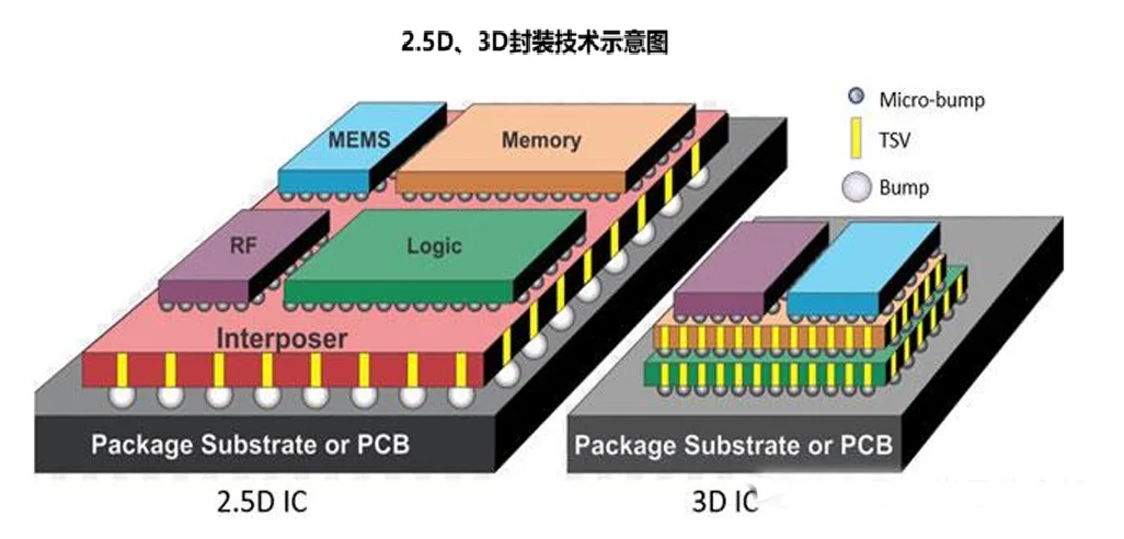
Schematic Diagram of 3D Packaging Technology
TSV Technology: Processes and Manufacturing Flow
TSV technology creates vertical signal pathways through the substrate, connecting the RDL (Redistribution Layer) at the top and bottom of the substrate, forming a 3D conductor pathway. Based on the sequence with front-end-of-line (FEOL) and back-end-of-line (BEOL) processes, TSV processes can be divided into three mainstream manufacturing flows: ViaFirst, ViaMiddle, and ViaLast.
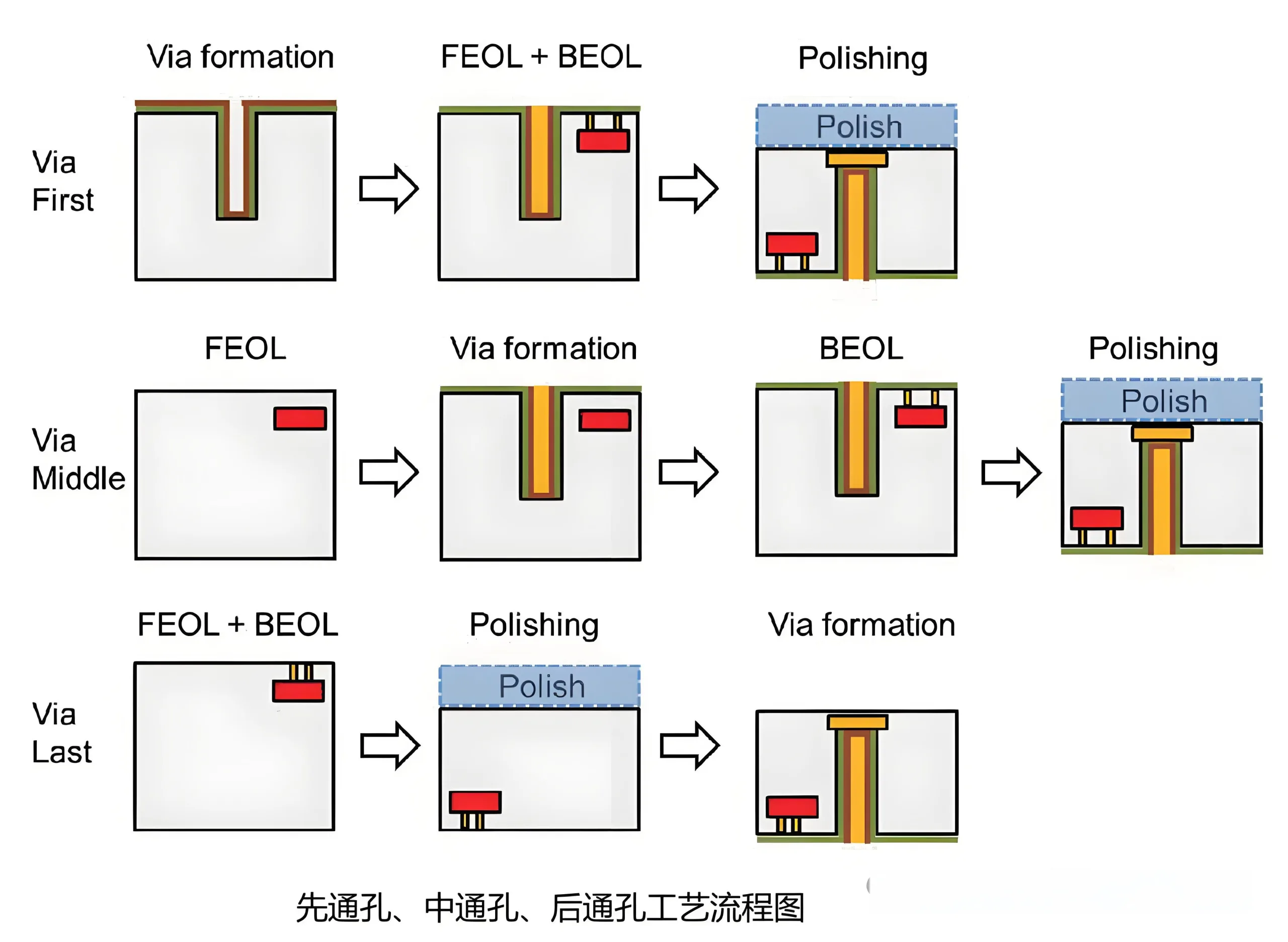
TSV Technology: Process and Manufacturing Procedure
Via Etching Process
The via etching process is crucial for manufacturing TSV structures. ตอนนี้, there are four mainstream etching processes: Deep Reactive Ion Etching (DRIE), wet etching, Photo-Assisted Electrochemical Etching (PAECE), and laser drilling.
DRIE
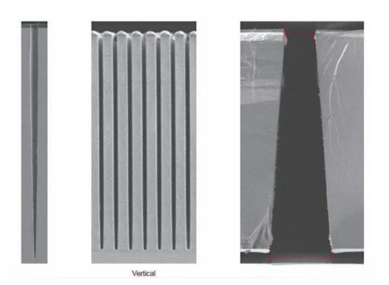
The high aspect ratio through-hole formed by DRIE process etching
The most commonly used TSV etching process for achieving high aspect ratio via structures. The Bosch process, an improved version of DRIE, uses SF6 and C4F8 gases for sidewall passivation protection, suitable for etching high aspect ratio vias. อย่างไรก็ตาม, DRIE processes result in poor sidewall smoothness, forming scallop-shaped defects.
Wet Etching
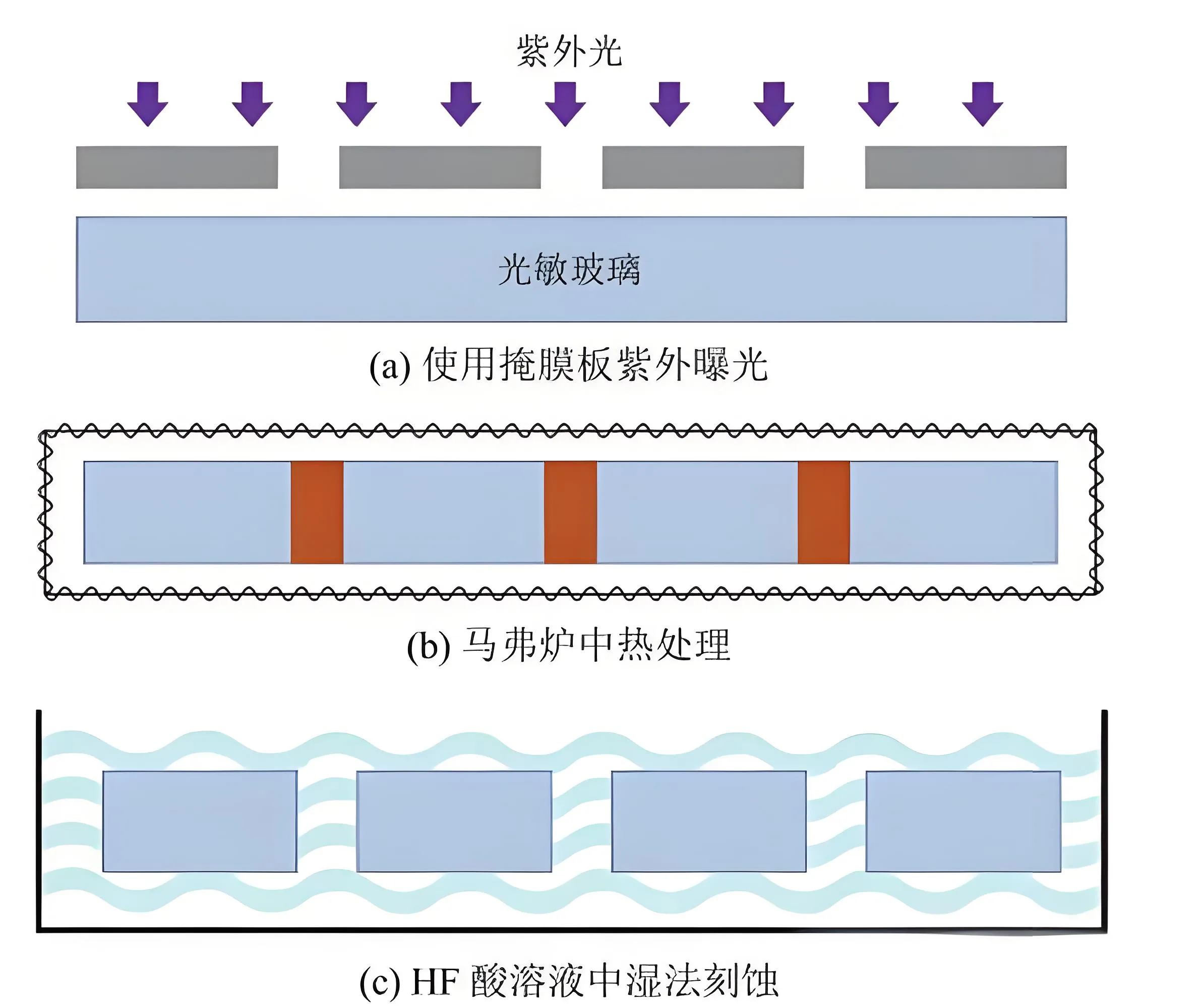
Wet etching
Combines a mask with chemical etching, making the process simple and suitable for low-cost mass production. อย่างไรก็ตาม, due to the influence of silicon wafer crystallographic orientation, the etched vias are not vertical, limiting its application.
PAECE
Utilizes ultraviolet light to accelerate the generation of electron-hole pairs, accelerating the electrochemical etching process, suitable for etching ultra-high aspect ratio via structures, but with weaker etch depth controllability.
Laser Drilling
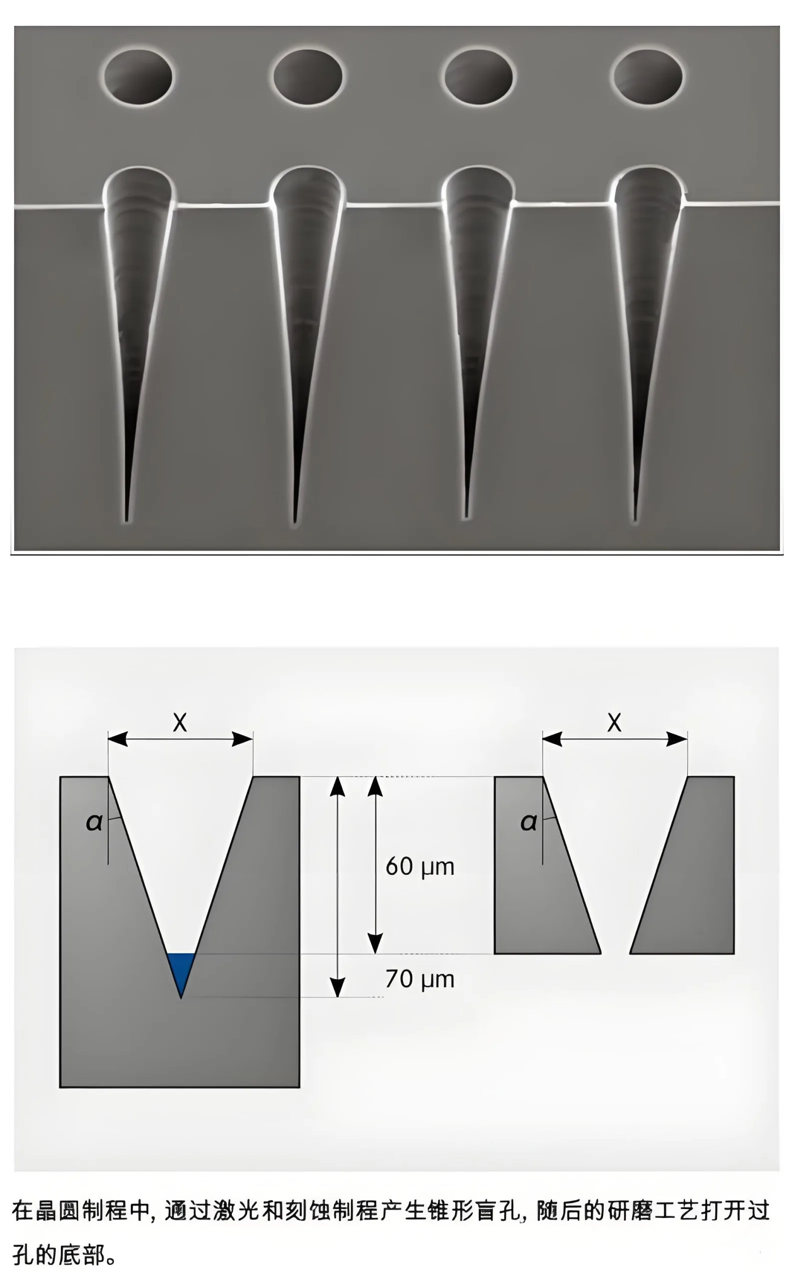
Laser Drilling
Uses high-energy laser beams to melt and evaporate materials in the specified area, forming high aspect ratio, vertically sidewall vias, but the hole walls are susceptible to thermal damage affecting reliability.

Through-Silicon Via Technology
Liner Deposition Process
The liner deposition process is performed after via etching. The deposited liner layer, typically an oxide such as SiO2, serves to isolate direct current leakage. The deposition process must meet the breakdown voltage requirements of the insulating layer and ensure strong consistency and good adhesion between layers.
พีอีซีวีดี
Used to deposit SiO2 or SiNx as the insulating layer, suitable for ViaMiddle and ViaLast processes, ensuring compatibility with BEOL materials.
ALD
Deposits Al2O3 to obtain a denser insulating layer.
Metal Fill Process
The TSV fill process determines TSV quality, with electroplated copper being the mainstream material. Based on differences in electroplating rate distribution, it can be divided into sub-conformal, conformal, super-conformal, and bottom-up electroplating methods.
Conformal Electroplating
Ensures uniform replenishment of Cu ions, making the electroplating rate basically consistent at all positions within the via, leaving only one seam inside.
Super-Conformal Electroplating
By controlling the supply of Cu ions, the bottom filling rate is slightly higher than other positions, eliminating seams and achieving void-free filling.
Bottom-Up Electroplating
The electroplating rate is suppressed to zero except at the bottom, gradually electroplating from the bottom to the top, reducing electroplating time.
RDL Process Technology
RDL technology is an essential basic technology in 3D packaging, used to create metal interconnects for port reassignment or interconnection between packages. There are two mainstream RDL processes: based on photosensitive polymers and Cu damascene.
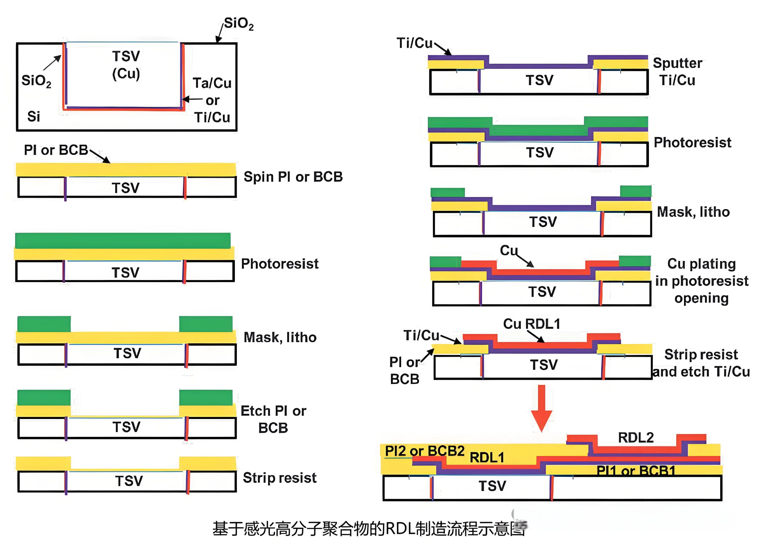
RDL process flow diagram
RDL Process Based on Photosensitive Polymers
Involves spin-coating PI or BCB resin, photolithography, การแกะสลัก, PVD sputtering of Ti/Cu barrier/seed layers, and combining photolithography with Cu electroplating to manufacture RDL.
Cu Damascene Process
First deposits SiO2 or Si3N4 as the insulating layer, forms windows through photolithography and etching, sputters Ti/Cu, and uses CMP to reduce to the desired thickness.
IPD Process and TGV Technology: A New Path for 3D Passive Devices
The Integrated Passive Device (IPD) process forms a library of passive devices that can be called upon as needed by integrating passive devices onto a separate substrate. IPD offers the advantages of low cost and high flexibility, especially suitable for TSV 3D passive device manufacturing. IPD can use various substrate materials, including Si, GaN, Al2O3 ceramics, glass substrates, ฯลฯ, expanding design flexibility.
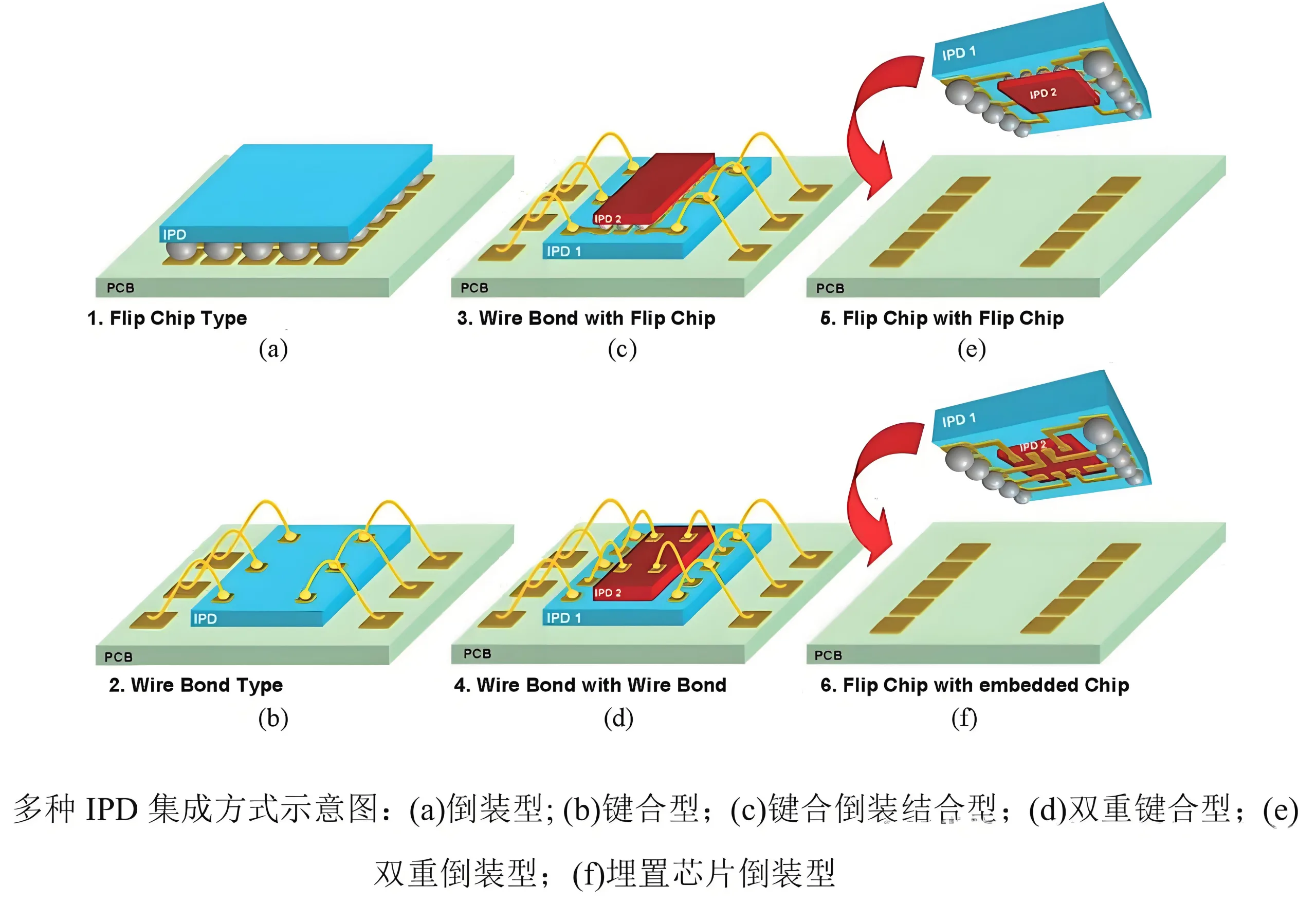
Integrated Passive Device Process
3D inductors manufactured based on IPD and TGV processes exhibit superior insulation characteristics due to the much higher resistivity of glass substrates compared to conventional semiconductor materials, resulting in low insertion loss. นอกจากนี้, MIM capacitors can be fabricated on glass substrate IPDs, interconnected with TGV 3D inductors to form 3D passive filter structures.
บทสรุป
As key technologies in 3D packaging, TSV and TGV technologies have not only driven innovations in semiconductor packaging technology but also provided strong support for the miniaturization, high-density, and high-performance of electronic products. With continuous technological development, TSV and TGV will play an increasingly important role in future electronic products, ushering in a new era of 3D packaging. Through continuous exploration and innovation, we have reason to believe that TSV and TGV technologies will bring humans a smarter, more convenient, and efficient electronic lifestyle.
 โลโก้ UGPCB


