
พีซีบีพิเศษ
UGPCB Special PCB Solutions: Empowering High-End Electronic System Innovation with Cross-Material Integration Technology
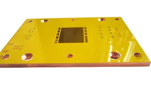
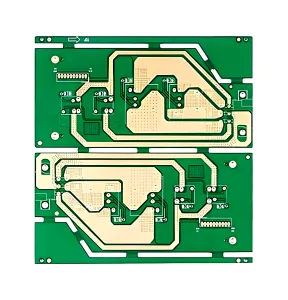
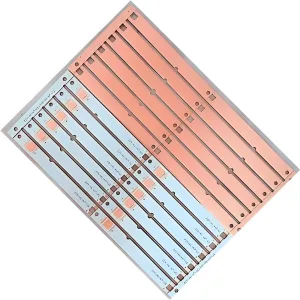
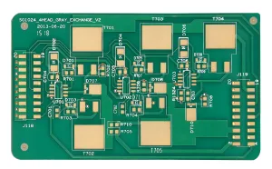
In the era of rapid development of 5G communication, aerospace, and smart industrial equipment, UGPCB, as a global leader in special PCB technology, showcases its customized circuit board solutions for extreme environments and complex scenarios through the “พีซีบีพิเศษ” section of its corporate website. With over a decade of industry expertise, we provide innovative products that break traditional PCB performance limits for military, ทางการแพทย์, automotive electronics, and other fields by leveraging multi-material collaborative design, high-precision manufacturing processes, and full-cycle reliability verification.
Core Technological Advantages: Building Professional Barriers for Special PCBs
1. Cross-Material Collaborative Design Platform
• High-Frequency Hybrid Layer Technology: Innovatively integrates PCB materials such as FR-4, โรเจอร์ส, and ceramic substrates, achieving a 35% cost reduction in the radio frequency range while ensuring signal integrity in millimeter-wave/terahertz bands through dynamic dielectric constant matching (Dk±0.03@40GHz).
• Extreme Environmental Adaptability: Employs low-CTE metal bases (aluminum/copper) and PTFE composites, passing 2000 thermal cycle tests (-65℃↔200℃) under GJB 548B standards to meet aerospace-grade temperature and impact resistance requirements.
2. High-Density Signal Integrity Assurance
• 3D Electromagnetic Compatibility Architecture: Integrates metallized shielding cavities (isolation >70dB@10GHz) and stepped grounding designs to meet stringent EMC standards like MIL-STD-461G/DO-160.
• Ultra-Precision PCB Impedance Control: Based on Ansys HFSS full-wave simulation, achieves ±3% impedance tolerance for 112G PAM4 signals, power integrity impedance <1mΩ, supporting PCIe 6.0/USB4 specifications.
3. Precision Manufacturing Process System
• Nano-Scale Laser Processing: Picosecond laser drilling technology enables ±5μm aperture tolerance, supporting 0.08mm ultra-micro holes and 50μm line width/spacing, increasing wiring density by 4 ครั้ง.
• Vacuum Hot Press Molding: Segmented pressure control eliminates interfacial delamination risks between heterogeneous materials, ensuring ±2% laminate thickness uniformity and consistent high-frequency performance.
Typical Application Scenarios and Performance Benchmarks
• Satellite Communication Payload Systems: 28-layer aluminum-based hybrid PCB (Rogers RO3003™ + metal core) supporting Ka-band phased array antenna EIRP>60dBm, certified by IPC-6012DS aerospace reliability standards.
• New Energy Vehicle Electric Drive Control: 18-layer thick copper PCB (6oz inner layer) with 3kV voltage resistance/150℃ temperature resistance, meeting AEC-Q200 Grade 0 standards and supporting SiC power module integration.
• High-End Medical Imaging Equipment: 10-layer ceramic-based PCB with dielectric loss Df≤0.0015@10GHz, compatible with MRI strong magnetic field environments, and ISO 13485 medical electronics certified.
Full-Cycle PCB Service System and Certification Assurance
• Collaborative Design Support: Provides Cadence Allegro/SI/PI simulation, Flotherm® thermodynamic analysis, and HALT accelerated life testing (40G vibration/three-proof salt spray environment).
• Rapid Response Delivery: 5-day delivery for 12-layer special PCB samples, supports ODB++/IPC-2581 intelligent DFM review, and 15-day mass production for complex HDI structures.
• Military-Grade Quality Control System: 100% compliance with IPC-6012E Class 3A standards, double-certified by NADCAP military and AS9100D aerospace quality management systems.
Reasons to Choose UGPCB
- Technological Foresight: Over 300 patented technologies covering cutting-edge fields like millimeter-wave radar and quantum communication, continuously defining industry standards.
- Cost Optimization: Intelligent panelization algorithms increase material utilization by 20%, hybrid layer solutions reduce customer BOM costs by 30%-50%.
- Zero-Risk Mass Production: Fully automated AOI+3D X-ray inspection, stable mass production yield >99.8%, supporting million-unit order delivery.
Get Your UGPCB Special PCB Exclusive Solution Now
Visit the “พีซีบีพิเศษ” product section on our corporate website, submit your requirements to receive for free:
✅ Customized cross-material layer stack simulation report
✅ Extreme environment reliability pre-test data
✅ 24-hour rapid quotation and technical support
 โลโก้ UGPCB


วีแชท
สแกนรหัส QR ด้วย WeChat