
Introduction to the 12 Layers 3+N+3 HDI Communication PCB
ภาพรวมผลิตภัณฑ์
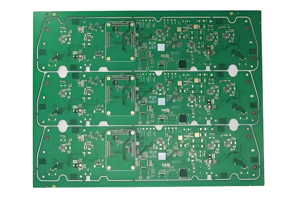
The 12 Layers 3+N+3 Communication PCB is a high-density interconnect (HDI) printed circuit board designed specifically for communication products. It features a twelve-layer construction with a thickness of 1.2mm, ensuring durability and compactness suitable for advanced communication devices.
Design Requirements
This main board adheres to stringent design requirements, including a minimum trace and space of 2.5mil/2.5mil. These specifications ensure precise connectivity and efficient miniaturization, crucial for today’s slim and powerful communication devices.
หลักการทำงาน
The 12 Layers 3+N+3 HDI Communication PCB operates based on advanced HDI PCB technology, allowing for intricate component placement and signal routing within a limited space. The board utilizes high-frequency switching and optimized power distribution to manage the complex functionalities of communication devices.
การใช้งาน
Primarily used as the core platform in communication products, this main board integrates various electronic components, processors, memory modules, and communication interfaces. It facilitates seamless operation and enhanced performance for communication devices.
Classification and Materials
Board Classification
Classified as an HDI PCB, ที่ 12 Layers 3+N+3 HDI Communication PCB stands out due to its multi-layer structure and fine pitch capabilities, making it ideal for high-performance communication devices.
องค์ประกอบของวัสดุ
Constructed from TU872slk material, known for its excellent heat resistance and mechanical stability, the board ensures reliable operation even under demanding conditions. The copper thickness of 0.5OZ further enhances conductivity and signal integrity.
ลักษณะประสิทธิภาพ
With its blue or white color options, the board not only meets aesthetic preferences but also signifies different insulation levels or manufacturing batches. Surface treatments like Immersion Gold provide superior solderability and protection against oxidation.
Structural Features and Production Process
Structural Design
The 3+6+3 layer arrangement in the HDI PCB structure optimizes space utilization and thermal management. This configuration supports complex routing needs without compromising signal quality or board strength.
Production Flow
Manufacturing begins with material selection, followed by layer pressing, การขุดเจาะ (including laser drilling for fine holes), plating, การแกะสลัก, and final surface finish application. Each step is meticulously controlled to ensure the highest quality standards are met.
ใช้สถานการณ์กรณี
Typical Use Cases
In practical terms, ที่ 12 Layers 3+N+3 HDI Communication PCB is employed in flagship communication products requiring top-tier processing power, extended battery life, and advanced features such as 5G connectivity. It also finds applications in gaming phones where thermal management and high-speed data transfer are paramount.
บทสรุป
โดยสรุป, ที่ 12 Layers 3+N+3 HDI Communication PCB represents a pinnacle of technological advancement in mobile device manufacturing. Its sophisticated design, adherence to strict specifications, and use of premium materials make it an indispensable component for next-generation mobile electronics.


