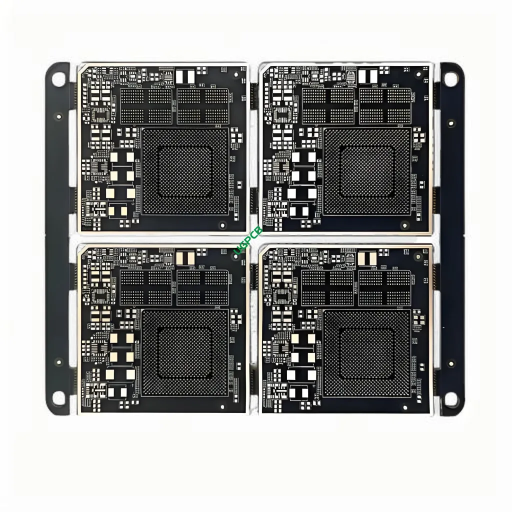
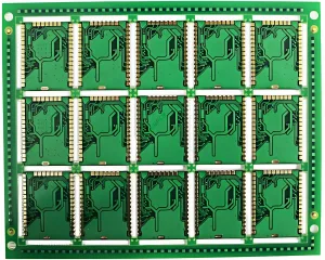
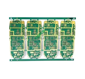
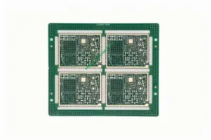
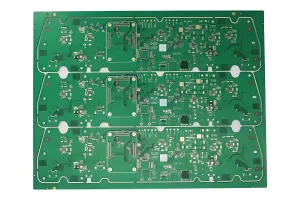
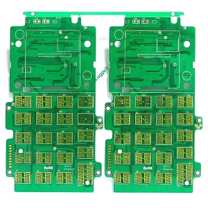
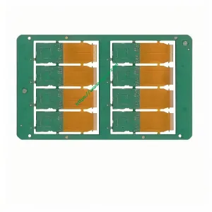
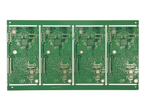
1+N+1 HDI PCB for Digital Product Overview
The 1+N+1 HDI PCB is a high-density interconnect printed circuit board designed specifically for digital products. It features six layers, with the construction pattern being 1+4+1. The material used for this PCB is SY S1000-2 FR4, and it has a finished thickness of 1.2mm. The copper thickness is 0.5OZ, and the surface treatment applied is immersion gold. This PCB can accommodate trace/space as small as 4mil/4mil and laser holes as tiny as 0.1mm.
Definition
HDI PCB stands for High Density Interconnect Printed Circuit Board. It’s a type of PCB that allows more components to be packed into a smaller area than traditional PCBs by using microvias or blind/buried vias which significantly reduce the need for space between layers.
Design Requirements
The design requirements for the 1+N+1 HDI PCB include a minimum trace/space of 4mil/4mil and a minimum hole size of 0.1mm. These specifications allow for intricate designs and complex circuitry within a compact form factor.
หลักการทำงาน
The working principle of an HDI PCB involves the use of advanced fabrication techniques to create multiple layers of conductive material separated by insulating layers. These layers are interconnected through microvias, allowing signals to travel between them without taking up much space.
Purpose
The primary purpose of the 1+N+1 HDI PCB is to provide a reliable platform for mounting and connecting electronic components in digital products. Its high density and small size make it ideal for applications where space is limited but performance is paramount.
การจำแนกประเภท
Based on its structure and application, the 1+N+1 HDI PCB can be classified as a high-density interconnect printed circuit board designed specifically for digital products.
Materials
The main material used in the construction of this PCB is SY S1000-2 FR4, a flame-resistant glass-epoxy laminate commonly used in PCB manufacturing due to its excellent electrical properties and thermal stability.
Performance
The performance of the 1+N+1 HDI PCB is characterized by its ability to handle high frequencies and large currents, making it suitable for demanding digital product applications. Its immersion gold surface treatment also provides excellent solderability and corrosion resistance.
Structure
The structure of the 1+N+1 HDI PCB consists of six layers: one top layer, four inner layers, and one bottom layer. The inner layers are connected through microvias, which are small holes that allow for denser circuitry without increasing the overall size of the board.
คุณสมบัติ
Some notable features of the 1+N+1 HDI PCB include its high density, ขนาดเล็ก, and ability to handle complex circuitry. Its immersion gold surface treatment also enhances its durability and solderability.
กระบวนการผลิต
The production process of the 1+N+1 HDI PCB involves several steps, including layout design, photolithography, การแกะสลัก, การขุดเจาะ, plating, and inspection. Each step requires precision and attention to detail to ensure the final product meets the specified standards and requirements.
Use Cases
The 1+N+1 HDI PCB is used in a variety of digital products where space is at a premium but performance is crucial. This includes smartphones, แท็บเล็ต, laptops, and other portable electronic devices. Its high density and small size make it an ideal choice for these applications.
 โลโก้ UGPCB

