Introduction to the 6L 2+N+2 HDI Product
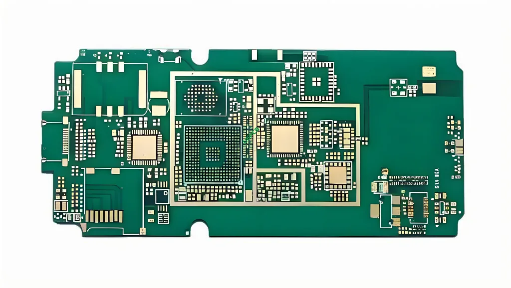
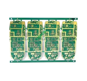
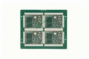
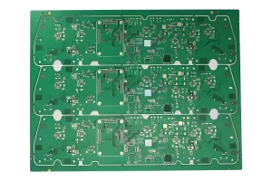
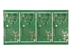
The 6L 2+N+2 HDI product is a high-density interconnect (HDI) printed circuit board (พีซีบี) designed for advanced communication applications. This guide provides a comprehensive overview of its specifications, design requirements, working principles, usage scenarios, and manufacturing process.
Definition and Design Requirements
แบบอย่าง: 6L 2+N+2 HDI
This model refers to a six-layer PCB with two internal power layers (2+n), two external signal layers, and two additional high-density interconnect layers. The ‘N’ represents the number of internal signal layers, which can vary depending on specific application needs.
วัสดุ: FR-4 ITEQ IT180A
The base material used is FR-4 ITEQ IT180A, known for its excellent thermal stability, ความแข็งแรงเชิงกล, and flame resistance.
Layer Composition: 6L 2+N+2 HDI
This indicates a six-layer structure with specific layer arrangements for optimized signal integrity and power distribution.
ความหนาสำเร็จรูป: 1.0มม
The total thickness of the finished PCB is 1.0 millimeters, ensuring durability while maintaining flexibility for various applications.
ความหนาของทองแดง: Inner 1OZ, Outer 0.5OZ
The copper traces on inner layers have a thickness of 1 ออนซ์ (ออนซ์), whereas the outer layers feature a thinner 0.5 oz copper, balancing conductivity and space efficiency.
Working Principle and Purpose
การรักษาพื้นผิว: ทองแช่ + OSP
To enhance solderability and protect against oxidation, the PCB undergoes immersion gold plating combined with Organic Solderability Preservatives (OSP).
Minimum Trace/Space: 2.5mil/2.5mil
The PCB supports fine pitch components with a minimum trace width and spacing of 2.5 mils (thousandths of an inch), facilitating compact designs without compromising performance.
Min Hole Diameter: Mechanical Hole 0.2mm, Laser Hole 0.1mm
It accommodates small components through mechanical drilling down to 0.2mm and even finer laser-drilled holes at 0.1mm, enabling high-density integration.
แอปพลิเคชัน: Communication Products PCB
Primarily tailored for communication devices, this PCB ensures reliable signal transmission and minimal interference, crucial for maintaining clear and consistent data flow in telecommunications systems.
Classification and Materials
การจำแนกประเภท: High-Density Interconnect (HDI) พีซีบี
As an HDI PCB, it belongs to a category of boards specifically engineered for complex electronic devices that require intricate routing and component placement.
วัสดุ: FR-4 ITEQ IT180A
FR-4 is a composite material widely used in PCB manufacturing due to its balance of electrical properties, thermal resistance, and cost-effectiveness. The specific grade, ITEQ IT180A, further ensures consistent quality and performance.
Performance and Structure
Performance: Superior Signal Integrity
With its carefully designed layer stack and use of high-quality materials, the 6L 2+N+2 HDI PCB guarantees exceptional signal integrity, reducing crosstalk and electromagnetic interference (อีเอ็มไอ).
Structure: Multi-Layer Arrangement
The structure comprises multiple layers strategically arranged to separate power planes from signal layers, minimizing noise and enhancing overall circuit performance. The inclusion of HDI technology allows for more intricate designs within a compact form factor.
Features and Production Process
กระบวนการพิเศษ: Half Hole Package Edge
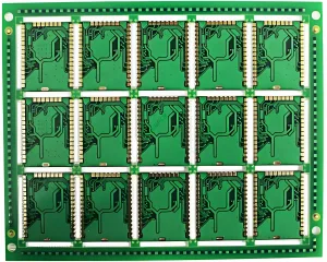
A unique feature involves the use of half hole packaging along the edge, which optimizes space utilization and improves connectivity options for edge-mounted components or connectors.
กระบวนการผลิต: Precision Manufacturing
Manufacturing begins with material selection and continues through precision drilling, plating, and laminating processes. Each step is meticulously controlled to ensure adherence to tight tolerances and high standards of quality.
Typical Use Cases and Scenarios
Typical Use Cases: Telecommunication Equipment
Commonly employed in telecommunication infrastructure such as routers, switches, and base stations, where high-speed data transfer and signal reliability are paramount.
Usage Scenarios: High-Frequency Applications
Suitable for applications involving high-frequency signals, including wireless communication modules and RF components, where minimizing signal loss and maximizing bandwidth efficiency are critical.
สรุปแล้ว, the 6L 2+N+2 HDI PCB stands out as a sophisticated solution for demanding communication product requirements, offering unparalleled density, performance, and reliability tailored to modern telecommunications needs.
 โลโก้ UGPCB

