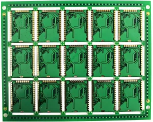
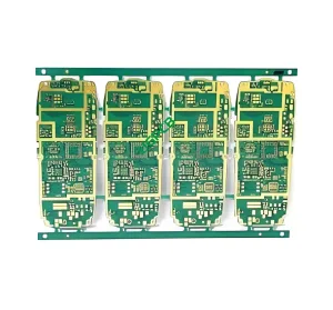
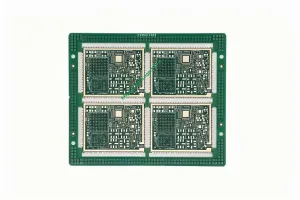
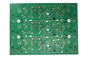
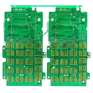
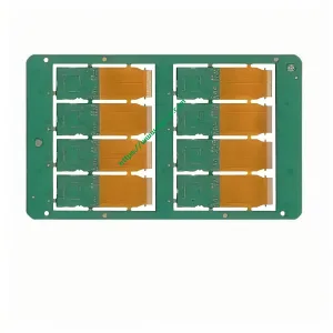
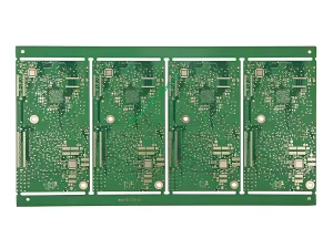
About Smart phone main board PCB (เอชดีไอ พีซีบี) lead time:
12 layers 3-level HDI PCB,15-18 days for proofing, 15-25 days for batches, special multi-layer PCB proofing and special negotiation for batch delivery, UGPCB can make Smart phone main board PCB(เอชดีไอ พีซีบี) fast prototype fabrication and the fastest delivery time for 12-layer 3-level HD UGPCB is 7 วัน.
For the Smart phone main board PCB(เอชดีไอ พีซีบี) process capability of UGPCB, please click HDI PCB Technics Capacity.
UGPCB Circuits Limited(UGPCB®) is a high-tech enterprise focus on the R&D and production of precision PCB prototype. UGPCB independently developed the first PCB Automatic Quotation System(PAQS) in the industry, which automatically connected our PCB factory to realize intelligent service and PCB prototype rapid fabrication. Our ultimate goal is to build an Internet + อุตสาหกรรม 4.0 intelligent PCB factory cluster to provide professional PCB technology and PCB prototype fabrication services for customers.
UGPCB® manufactures microwave radio frequency(RF) พีซีบี, hybrid high frequency PCB, (1-70ชั้น) PCB หลายชั้น, เอชดีไอ พีซีบี, rigid-flex PCB, metal based PCB, ceramic PCB. We have deep research on PCB with special requirements such as blind buried hole PCB, back drilling PCB, step slot PCB, IC carrier PCB, ultra thick copper PCB, ฯลฯ
 โลโก้ UGPCB


