
Introduction to Wireless Charging PCB
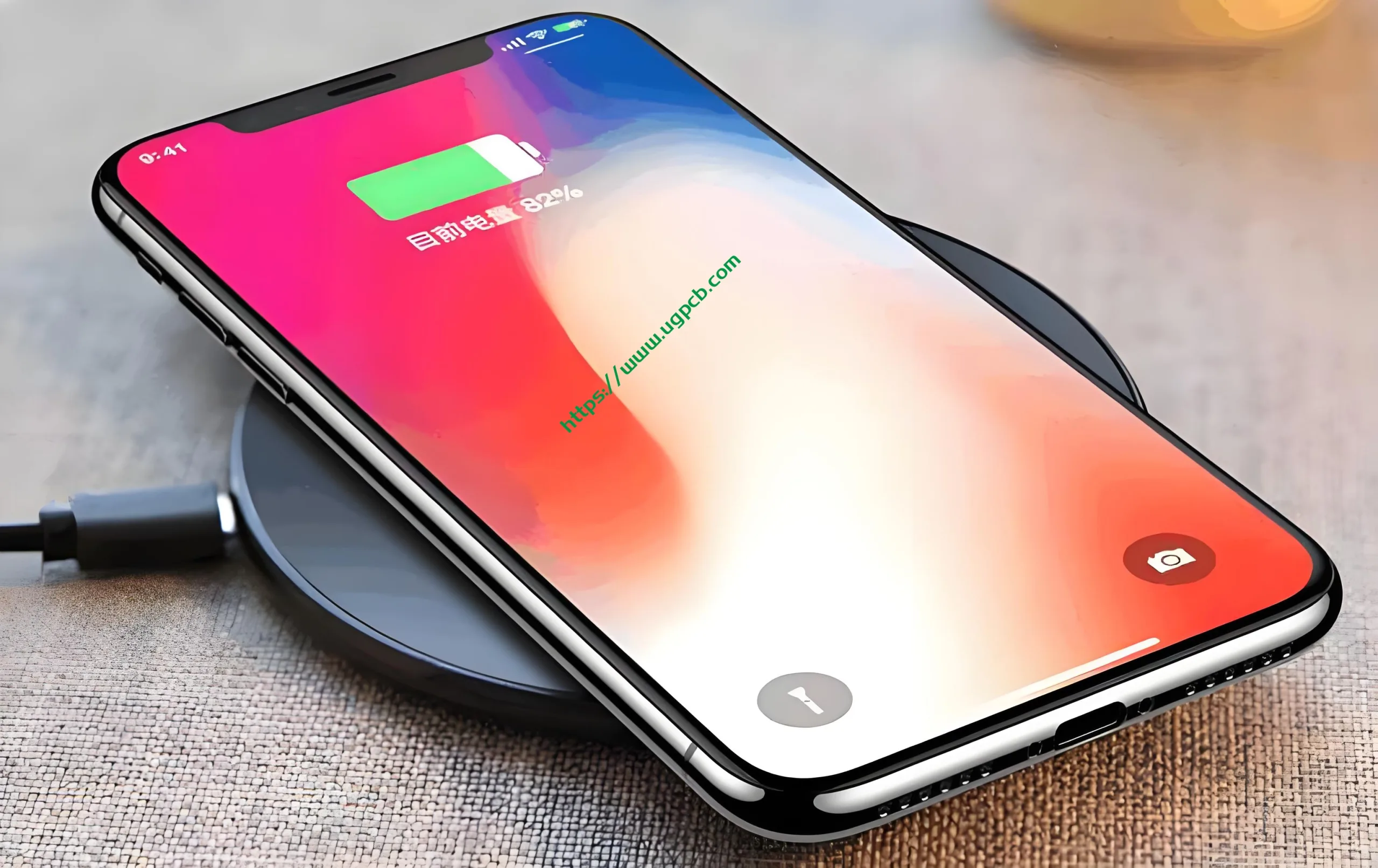
A Wireless Charging PCB, also known as an inductive charging circuit board, is a specialized printed circuit board designed for wireless power transfer. It enables devices such as smartphones, แท็บเล็ต, and other electronic gadgets to be charged without the need for physical connectors.
หลักการทำงาน
Wireless charging technology operates on the principle of electromagnetic induction. The transmitter coil generates an alternating electromagnetic field that induces a current in the receiver coil, thus transferring energy from the charger to the device.
การใช้งาน
Wireless Charging PCBs are widely used in consumer electronics for charging devices like mobile phones, smartwatches, earbuds, and even electric toothbrushes. They offer convenience, ease of use, and reduced wear and tear on charging ports.
Types of Wireless Charging PCBs
There are two main types of wireless charging technologies:
- Qi Standard: The most common and widely adopted wireless charging standard.
- PMA (Power Matters Alliance): Another popular standard, often found in older devices.
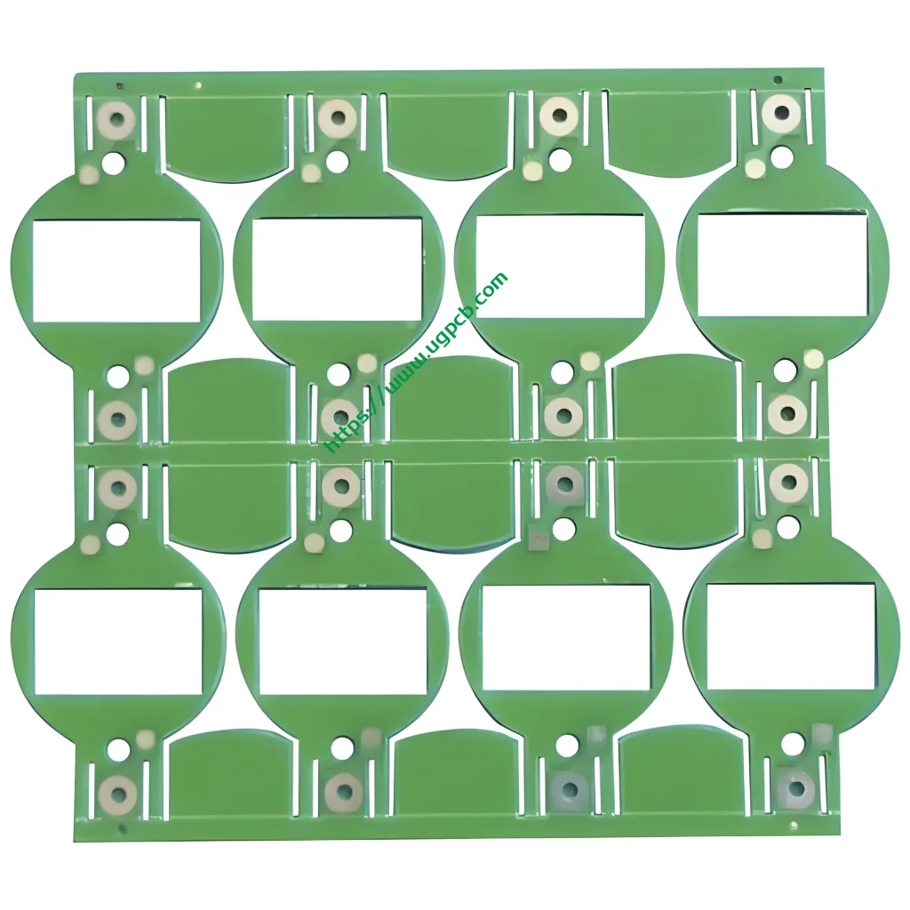
Material and Construction
- วัสดุ: S1000-2, a high-quality epoxy material.
- เลเยอร์: 6 ชั้น, providing robustness and better signal integrity.
- สี: Available in green or white.
- ความหนาสำเร็จรูป: 1.2มม, ensuring durability while being slim.
- ความหนาของทองแดง: 2ออนซ์, which offers good conductivity.
- การรักษาพื้นผิว: Immersion gold with a thickness of at least 2U”, enhancing corrosion resistance and solderability.
- Copper Thickness in Hole: 35UM, ensuring strong connections.
- Minimum Aperture: 0.4มม, allowing for fine detail work.
ลักษณะประสิทธิภาพ
Wireless Charging PCBs are designed to efficiently transfer power with minimal loss. They support fast charging capabilities and are built to withstand repeated usage over time. The immersion gold finish ensures long-lasting performance and reliability.
คุณสมบัติเชิงโครงสร้าง
The structure of a Wireless Charging PCB includes multiple layers of copper traces sandwiched between layers of substrate material. This multilayer design helps in managing heat dissipation and improving electrical performance. The PCB is coated with a protective layer to prevent damage and ensure longevity.
กระบวนการผลิต
The production of a Wireless Charging PCB involves several steps:
- ออกแบบ: Using specialized software to create the circuit layout.
- การแกะสลัก: Removing excess copper to form the desired patterns.
- การเคลือบ: Combining multiple layers together.
- Plating: Adding a thin layer of metal to improve connectivity.
- Inspection: Ensuring the PCB meets quality standards.
- Assembly: Mounting components onto the PCB.
- การทดสอบ: Verifying functionality and performance.
Use Cases
Wireless Charging PCBs are used in various applications including:
- Consumer Electronics: Mobile phones, แท็บเล็ต, smartwatches.
- Automotive: In-car charging systems for smartphones.
- Medical Devices: Portable medical equipment.
- Wearables: Fitness trackers, smart rings.
สรุปแล้ว, Wireless Charging PCBs represent a significant advancement in charging technology, offering convenience, efficiency, และความทนทาน. Their widespread adoption across different industries highlights their versatility and importance in modern electronic devices.


